EVAL-ADF4154EBZ1 Analog Devices Inc, EVAL-ADF4154EBZ1 Datasheet - Page 10
EVAL-ADF4154EBZ1
Manufacturer Part Number
EVAL-ADF4154EBZ1
Description
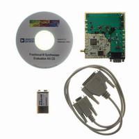
BOARD EVALUATION FOR ADF4154EB1
Manufacturer
Analog Devices Inc
Datasheet
1.ADF4154BRUZ.pdf
(24 pages)
Specifications of EVAL-ADF4154EBZ1
Main Purpose
Timing, Frequency Synthesizer
Embedded
No
Utilized Ic / Part
ADF4154
Primary Attributes
Single Fractional-N PLL
Secondary Attributes
19.2MHz PFD, Graphical User Interface
Lead Free Status / RoHS Status
Lead free / RoHS Compliant


ADF4154
MUXOUT AND LOCK DETECT
The output multiplexer on the ADF4154 allows the user to
access various internal points on the chip. The state of
MUXOUT is controlled by M3, M2, and M1 (see Table 8).
Figure 18 shows the MUXOUT section in block diagram form.
The N-channel, open-drain, analog lock detect should be
operated with an external pull-up resistor of 10 kΩ nominal.
When lock has been detected, the lock detect is high with
narrow low-going pulses.
ANALOG LOCK DETECT
INPUT SHIFT REGISTERS
The ADF4154 digital section includes a 4-bit R value, a 9-bit
RF N value, a 12-bit RF FRAC value, and a 12-bit interpolator
modulus value/fast-lock timer. Data is clocked MSB first into
the 24-bit shift register on each rising edge of CLK.
THREE-STATE OUTPUT
DIGITAL LOCK DETECT
FAST-LOCK CONTROL
R-DIVIDER OUTPUT
N-DIVIDER OUTPUT
LOGIC HIGH
LOGIC LOW
Figure 18. MUXOUT Schematic
MUX
CONTROL
DGND
DV
DD
MUXOUT
Rev. A | Page 10 of 24
Data is transferred from the shift register to one of four latches
on the rising edge of LE. The destination latch is determined by
the state of the two control bits (C2 and C1) in the shift register.
These are the two LSBs, DB1 and DB0, as shown in Figure 2.
The truth table for these bits is shown in Table 5. Table 6 shows
a summary of how the latches are programmed.
PROGRAM MODES
Table 5 through Table 9 show how to set up the program modes
in the ADF4154.
The ADF4154 programmable modulus is double buffered,
meaning that two events must occur before the part can use a
new modulus value. The first event is that the new modulus value
must be latched into the device by writing to the R-divider register,
and the second event is that a new write must be performed on
the N-divider register. Therefore, whenever the modulus value
is updated, the N-divider register must be written to so that the
modulus value is loaded correctly.
Table 5. C2 and C1 Truth Table
Control Bits
C2
0
0
1
1
0
1
C1
0
1
Data Latch
N-divider register
R-divider register
Control register
Noise and spur register
Related parts for EVAL-ADF4154EBZ1
Image
Part Number
Description
Manufacturer
Datasheet
Request
R

Part Number:
Description:
IC, ADJ LDO REG, 1.5V TO 5V 250mA MSOP-8
Manufacturer:
Vishay
Datasheet:

Part Number:
Description:
IC, ADJ LDO REG, 1.5V TO 5V 0.6A 8-TSSOP
Manufacturer:
Vishay
Datasheet:
Part Number:
Description:
IC, ADJ LDO REG, 1.5V TO 5V 250mA MSOP-8
Manufacturer:
Vishay
Datasheet:

Part Number:
Description:
IC ADJ LDO REG 1.5V TO 5V 150mA 5-SOT-23
Manufacturer:
Vishay
Datasheet:

Part Number:
Description:
BOARD EVAL AS1324-AD
Manufacturer:
austriamicrosystems
Datasheet:
Part Number:
Description:
IC, ADJ LDO REG, 1.5V TO 5V 0.6A 8-TSSOP
Manufacturer:
Vishay
Datasheet:

Part Number:
Description:
IC, ADJ LDO REG, 1.5V TO 5V, 0.3A, MSOP8
Manufacturer:
Vishay
Datasheet:
Part Number:
Description:
IC, ADJ LDO REG, 1.5V TO 5V, 0.3A, MSOP8
Manufacturer:
Vishay
Datasheet:
Part Number:
Description:
IC, ADJ LDO REG 1.215V TO 5V 0.3A MSOP-8
Manufacturer:
Vishay
Datasheet:
Part Number:
Description:
IC, ADJ LDO REG 1.215V TO 5V 0.3A MSOP-8
Manufacturer:
Vishay
Datasheet:

Part Number:
Description:
±1.7g Dual-Axis IMEMS Accelerometer Evaluation Board
Manufacturer:
Analog Devices Inc
Datasheet:

Part Number:
Description:
IC MULTIPLIER ANALOG 8-SOIC T/R
Manufacturer:
Analog Devices Inc
Datasheet:

Part Number:
Description:
IC ANALOG MULTIPLIER 8-DIP
Manufacturer:
Analog Devices Inc
Datasheet:
Part Number:
Description:
IC ANALOG MULTIPLIER 8-SOIC
Manufacturer:
Analog Devices Inc
Datasheet:
Part Number:
Description:
IC ANALOG MULTIPLIER 8-DIP
Manufacturer:
Analog Devices Inc
Datasheet: