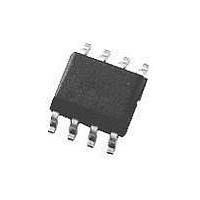
DS485M National Semiconductor, DS485M Datasheet - Page 2

DS485M
Manufacturer Part Number
DS485M
Description
IC, RS422/RS485 TRANSCEIVER 5.25V NSOIC8
Manufacturer
National Semiconductor
Datasheet
1.DS485M.pdf
(9 pages)
Specifications of DS485M
Device Type
Transceiver
Ic Interface Type
RS422, RS485
No. Of Drivers
1
Supply Voltage Range
4.75V To 5.25V
Driver Case Style
SOIC
No. Of Pins
8
Operating Temperature Range
0°C To +70°C
Lead Free Status / RoHS Status
Contains lead / RoHS non-compliant
Available stocks
Company
Part Number
Manufacturer
Quantity
Price
Part Number:
DS485M
Manufacturer:
NS/国半
Quantity:
20 000
Part Number:
DS485MX
Manufacturer:
NS/国半
Quantity:
20 000
Company:
Part Number:
DS485MX/NOPB
Manufacturer:
VTI
Quantity:
6 218
www.national.com
Symbol
V
V
∆V
V
V
∆V
V
V
I
I
V
∆V
V
V
I
R
I
I
I
I
IN1
IN2
OZR
CC
OSD1
OSD2
OSR
OD1
OD2
OD3
OC
IH
IL
TH
OH
OL
Absolute Maximum Ratings
If Military/Aerospace specified devices are required,
please contact the National Semiconductor Sales Office/
Distributors for availability and specifications.
Electrical Characteristics
Over Supply Voltage and Operating Temperature Ranges, unless otherwise specified (Notes 2, 3)
IN
Supply Voltage (V
Enable Input Voltage (RE*, DE)
Driver Input Voltage (DI)
Driver Output Voltage (A, B)
Receiver Input Voltage (A, B)
Receiver Output Voltage (RO)
Maximum Package Power Dissipation
Derate M Package 9.5 mW/˚C above +25˚C
Derate N Package 6.0 mW/˚C above +25˚C
Maximum Package Power Dissipation
OD
OC
TH
M Package
N Package
M Package
Differential Driver Output Voltage
Differential Driver Output Voltage
with Load
Change in Magnitude of Output
Differential Voltage
Differential Driver Output Voltage —
Full Load with Max V
Driver Common-Mode Output Voltage
Change in Magnitude of Common-Mode
Output Voltage
Input High Voltage
Input Low Voltage
Input Current
Input Current (Note 5)
DE = 0V, V
Receiver Differential Threshold Voltage
Receiver Input Hysteresis
Receiver Output High Voltage
Receiver Output Low Voltage
TRI-STATE Output Current at Receiver
Receiver Input Resistance
No-Load Supply Current (Note 6)
Driver Short Circuit Current, V
Driver Short Circuit Current, V
Receiver Short Circuit Current
CC
CC
)
= 0V or 5.25V
Parameter
CM
−0.5V to (V
−0.5V to (V
−0.5V to (V
O
O
@
@
= HIGH
= LOW
+25˚C
+70˚C
−14V to +14V
−14V to +14V
(Note 1)
CC
CC
CC
+ 0.5V)
+ 0.5V)
+ 0.5V)
1.19W
0.74W
0.76W
+12V
(No Load)
R
R
R
R1 = 54Ω, R2 = 375Ω
V
R
R
V
V
V
−7V ≤ V
V
I
I
0.4V ≤ V
−7V ≤ V
DE = V
DE = 0V, RE* = 0V or V
−7V ≤ V
−7V ≤ V
0V ≤ V
O
O
L
L
L
TEST
L
L
IN
IN
IN
CM
= −4 mA, V
= 4 mA, V
= 50Ω, (RS422), Figure 1
= 27Ω, (RS485), Figure 1
= 27Ω or 50Ω (Note 4)
= 27Ω or 50Ω, Figure 1
= 27Ω or 50Ω, Figure 1 (Note 4)
= 0V or V
= +12V
= −7V
= 0V
= −7V to +12V, Figure 5
O
CC
CM
IN
O
O
O
2
≤ V
, RE* = 0V or V
≤ +12V
≤ +12V
≤ +12V
≤ 2.4V
≤ +12V
CC
ID
Recommended Operating
Conditions
Conditions
CC
Storage Temperature Range
Lead Temperature Range
ESD (HBM)
ID
Supply Voltage (V
Operating Free Air
Temperature (T
Bus Common Mode Voltage
= −0.2V
N Package
(Soldering, 4 sec.)
= 0.2V
DS485
DS485T
CC
CC
A
)
CC
)
A, B
A, B
A, B
A, B
RE*
V
DE,
Pin
RO
RO
DI,
CC
+4.75 +5.0 +5.25
Min
−40
−7
0
−0.2
Min Typ
1.5
1.5
2.0
3.5
12
35
35
2
7
Typ
+25
+25
−65˚C to +150˚C
200
200
2.8
2.3
2.0
70
Max Units
+70
+85
+12
Max
−0.8
900
500
250
250
0.2
0.2
0.8
1.0
0.2
0.4
±
±
85
5
5
5
3
2
1
+260˚C
0.47W
≥2 kV
˚C
˚C
V
V
Units
mA
mA
mV
mA
mA
mA
kΩ
|V|
|V|
µA
µA
µA
µA
V
V
V
V
V
V
V
V
V
V


