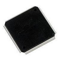
LFXP2-5E-5TN144C LATTICE SEMICONDUCTOR, LFXP2-5E-5TN144C Datasheet - Page 5

LFXP2-5E-5TN144C
Manufacturer Part Number
LFXP2-5E-5TN144C
Description
IC, LATTICEXP2 FPGA, 435MHZ, TQFP-144
Manufacturer
LATTICE SEMICONDUCTOR
Series
LatticeXP2r
Datasheet
1.LFXP2-5E-5TN144C.pdf
(93 pages)
Specifications of LFXP2-5E-5TN144C
No. Of Logic Blocks
5000
No. Of Macrocells
2500
Family Type
LatticeXP2
No. Of Speed Grades
5
No. Of I/o's
100
Clock Management
PLL
Total Ram Bits
166Kbit
Lead Free Status / RoHS Status
Lead free / RoHS Compliant
Available stocks
Company
Part Number
Manufacturer
Quantity
Price
Company:
Part Number:
LFXP2-5E-5TN144C
Manufacturer:
LATTICE
Quantity:
1 000
Company:
Part Number:
LFXP2-5E-5TN144C
Manufacturer:
Lattice
Quantity:
1 215
Company:
Part Number:
LFXP2-5E-5TN144C
Manufacturer:
Lattice Semiconductor Corporation
Quantity:
10 000
Part Number:
LFXP2-5E-5TN144C
Manufacturer:
LATTICE
Quantity:
20 000
Lattice Semiconductor
Figure 2-1. Simplified Block Diagram, LatticeXP2-17 Device (Top Level)
PFU Blocks
The core of the LatticeXP2 device is made up of logic blocks in two forms, PFUs and PFFs. PFUs can be pro-
grammed to perform logic, arithmetic, distributed RAM and distributed ROM functions. PFF blocks can be pro-
grammed to perform logic, arithmetic and ROM functions. Except where necessary, the remainder of this data
sheet will use the term PFU to refer to both PFU and PFF blocks.
Each PFU block consists of four interconnected slices, numbered Slice 0 through Slice 3, as shown in Figure 2-2.
All the interconnections to and from PFU blocks are from routing. There are 50 inputs and 23 outputs associated
with each PFU block.
Programmable
Function Units
(PFUs)
sysMEM Block
RAM
DSP Blocks
SPI Port
On-chip
Oscillator
sysCLOCK PLLs
2-2
Flexible Routing
sysIO Buffers,
Pre-Engineered Source
Synchronous Support
LatticeXP2 Family Data Sheet
Architecture
JTAG Port
Flash


