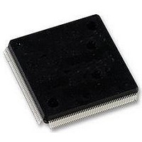
LFXP6C-5QN208C LATTICE SEMICONDUCTOR, LFXP6C-5QN208C Datasheet - Page 21

LFXP6C-5QN208C
Manufacturer Part Number
LFXP6C-5QN208C
Description
FPGA, 1.8V FLASH, INSTANT ON, SMD
Manufacturer
LATTICE SEMICONDUCTOR
Series
LatticeXPr
Datasheet
1.LFXP3C-3QN208C.pdf
(130 pages)
Specifications of LFXP6C-5QN208C
No. Of Logic Blocks
720
No. Of Macrocells
3000
Family Type
LatticeXP
No. Of Speed Grades
5
No. Of I/o's
142
Clock Management
PLL
Core Supply Voltage Range
1.71V To 3.465V
Lead Free Status / RoHS Status
Lead free / RoHS Compliant
Available stocks
Company
Part Number
Manufacturer
Quantity
Price
Company:
Part Number:
LFXP6C-5QN208C
Manufacturer:
Lattice Semiconductor Corporation
Quantity:
10 000
- Current page: 21 of 130
- Download datasheet (2Mb)
Lattice Semiconductor
Figure 2-21. Input Register DDR Waveforms
Figure 2-22. INDDRXB Primitive
Output Register Block
The output register block provides the ability to register signals from the core of the device before they are passed
to the sysIO buffers. The block contains a register for SDR operation that is combined with an additional latch for
DDR operation. Figure 2-23 shows the diagram of the Output Register Block.
In SDR mode, ONEG0 feeds one of the flip-flops that then feeds the output. The flip-flop can be configured as a D-
type or as a latch. In DDR mode, ONEG0 is fed into one register on the positive edge of the clock and OPOS0 is
latched. A multiplexer running off the same clock selects the correct register for feeding to the output (D0).
Figure 2-24 shows the design tool DDR primitives. The SDR output register has reset and clock enable available.
The additional register for DDR operation does not have reset or clock enable available.
(In DDR Mode)
Delayed
DQS
DQS
D0
D2
DI
DDRCLKPOL
A
ECLK
SCLK
LSR
CE
D
B
2-18
IDDRXB
C
B
A
QA
QB
D
LatticeXP Family Data Sheet
E
D
C
F
Architecture
Related parts for LFXP6C-5QN208C
Image
Part Number
Description
Manufacturer
Datasheet
Request
R

Part Number:
Description:
FPGA, 1.8V FLASH, INSTANT ON, SMD
Manufacturer:
LATTICE SEMICONDUCTOR
Datasheet:

Part Number:
Description:
IC FPGA 5.8KLUTS 188I/O 256-BGA
Manufacturer:
Lattice
Datasheet:

Part Number:
Description:
FPGA - Field Programmable Gate Array 5.8K LUTS 142 I/O
Manufacturer:
Lattice
Datasheet:

Part Number:
Description:
FPGA - Field Programmable Gate Array 5.8K LUTs 100 IO 1.8 /2.5/3.3V -4 Spd I
Manufacturer:
Lattice
Datasheet:

Part Number:
Description:
FPGA - Field Programmable Gate Array 5.8K LUTs 142 IO 1.8 /2.5/3.3V -4 Spd
Manufacturer:
Lattice
Datasheet:

Part Number:
Description:
FPGA - Field Programmable Gate Array 5.8K LUTs 188 I/O 1.8/2.5/3.3V -4 Spd
Manufacturer:
Lattice
Datasheet:
Part Number:
Description:
FPGA LatticeXP Family 6000 Cells 360MHz 130nm (CMOS) Technology 1.8V/2.5V/3.3V 256-Pin FBGA Tray
Manufacturer:
LATTICE SEMICONDUCTOR
Datasheet:
Part Number:
Description:
FPGA LatticeXP Family 6000 Cells 400MHz 130nm (CMOS) Technology 1.8V/2.5V/3.3V 256-Pin FBGA Tray
Manufacturer:
LATTICE SEMICONDUCTOR
Datasheet:

Part Number:
Description:
FPGA LatticeXP Family 6000 Cells 360MHz 130nm (CMOS) Technology 1.8V/2.5V/3.3V 208-Pin PQFP Tray
Manufacturer:
Lattice
Datasheet:

Part Number:
Description:
IC FPGA 5.8KLUTS 100I/O 144-TQFP
Manufacturer:
Lattice
Datasheet:

Part Number:
Description:
IC FPGA 5.8KLUTS 100I/O 144-TQFP
Manufacturer:
Lattice
Datasheet:

Part Number:
Description:
IC FPGA 5.8KLUTS 100I/O 144-TQFP
Manufacturer:
Lattice
Datasheet:

Part Number:
Description:
IC FPGA 5.8KLUTS 100I/O 144-TQFP
Manufacturer:
Lattice
Datasheet:


