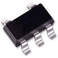
74LVC1G125GW NXP Semiconductors, 74LVC1G125GW Datasheet - Page 4

74LVC1G125GW
Manufacturer Part Number
74LVC1G125GW
Description
IC, LOGIC, 74LVC1G, BUFFER, UMT5
Manufacturer
NXP Semiconductors
Datasheet
1.74LVC1G125GW.pdf
(19 pages)
Specifications of 74LVC1G125GW
Supply Voltage Range
1.65V To 5.5V
Logic Case Style
SOT-353
No. Of Pins
5
Operating Temperature Range
-40°C To +125°C
Svhc
No SVHC (18-Jun-2010)
Logic Ic Base
RoHS Compliant
Package / Case
SOT-353
Logic Device Type
Buffer / Line Driver, Non Inverting
Rohs Compliant
Yes
Available stocks
Company
Part Number
Manufacturer
Quantity
Price
Company:
Part Number:
74LVC1G125GW
Manufacturer:
NXP
Quantity:
81 400
Company:
Part Number:
74LVC1G125GW
Manufacturer:
MACROBL
Quantity:
59
Part Number:
74LVC1G125GW
Manufacturer:
NXP/恩智浦
Quantity:
20 000
Company:
Part Number:
74LVC1G125GW(JB)
Manufacturer:
PHILIPS
Quantity:
140
Company:
Part Number:
74LVC1G125GW,125
Manufacturer:
NXP Semiconductors
Quantity:
4 300
Company:
Part Number:
74LVC1G125GWЈ¬125
Manufacturer:
NXP
Quantity:
15 000
NXP Semiconductors
8. Limiting values
Table 5.
In accordance with the Absolute Maximum Rating System (IEC 60134). Voltages are referenced to GND (ground = 0 V).
[1]
[2]
[3]
9. Recommended operating conditions
Table 6.
74LVC1G125
Product data sheet
Symbol
V
I
V
I
V
I
I
I
P
T
Symbol
V
V
V
T
t/V
IK
OK
O
CC
GND
stg
amb
CC
I
O
tot
CC
I
O
The input and output voltage ratings may be exceeded if the input and output current ratings are observed.
When V
For TSSOP5 and SC-74A packages: above 87.5 C the value of P
For XSON6 package: above 118 C the value of P
CC
Limiting values
Recommended operating conditions
Parameter
supply voltage
input clamping current
input voltage
output clamping current
output voltage
output current
supply current
ground current
total power dissipation
storage temperature
Parameter
supply voltage
input voltage
output voltage
ambient temperature
input transition rise and fall rate
= 0 V (Power-down mode), the output voltage can be 5.5 V in normal operation.
All information provided in this document is subject to legal disclaimers.
V
V
Active mode
V
Conditions
Power-down mode
T
Conditions
Active mode
V
V
V
amb
I
O
O
Rev. 9 — 29 December 2010
tot
< 0 V
CC
CC
CC
> V
= 0 V to V
derates linearly with 7.8 mW/K.
= 40 C to +125 C
= 0 V; Power-down mode
= 1.65 V to 2.7 V
= 2.7 V to 5.5 V
CC
or V
CC
O
< 0 V
tot
derates linearly with 4.0 mW/K.
[1][2]
[1][2]
[1]
[3]
Min
1.65
0
0
0
40
-
-
Min
0.5
50
0.5
-
0.5
0.5
-
-
100
-
65
Bus buffer/line driver; 3-state
74LVC1G125
Typ
-
-
-
-
-
-
-
Max
+6.5
-
+6.5
50
V
+6.5
50
100
-
250
+150
CC
© NXP B.V. 2010. All rights reserved.
V
Max
5.5
5.5
5.5
+125
20
10
+ 0.5
CC
Unit
V
V
V
V
C
ns/V
ns/V
Unit
V
mA
V
mA
V
V
mA
mA
mA
mW
C
4 of 19


