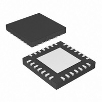
PIC16F1827-I/MV Microchip Technology, PIC16F1827-I/MV Datasheet - Page 212

PIC16F1827-I/MV
Manufacturer Part Number
PIC16F1827-I/MV
Description
IC, 8BIT MCU, PIC16F, 32MHZ, QFN-28
Manufacturer
Microchip Technology
Series
PIC® XLP™ 16Fr
Datasheets
1.PIC16F722-ISS.pdf
(8 pages)
2.PIC16F1826-IP.pdf
(406 pages)
3.PIC16F1826-IP.pdf
(12 pages)
4.PIC16F1826-IP.pdf
(8 pages)
5.PIC16F1826-IP.pdf
(40 pages)
6.PIC16LF1827-ISS.pdf
(400 pages)
Specifications of PIC16F1827-I/MV
Controller Family/series
PIC16F
Eeprom Memory Size
256Byte
Ram Memory Size
384Byte
Cpu Speed
32MHz
No. Of Timers
5
Interface
EUSART, I2C, SPI
Core Size
8 Bit
Program Memory Size
4kWords
Core Processor
PIC
Speed
32MHz
Connectivity
I²C, SPI, UART/USART
Peripherals
Brown-out Detect/Reset, POR, PWM, WDT
Number Of I /o
16
Program Memory Type
FLASH
Eeprom Size
256 x 8
Ram Size
384 x 8
Voltage - Supply (vcc/vdd)
1.8 V ~ 5.5 V
Data Converters
A/D 12x10b
Oscillator Type
Internal
Operating Temperature
-40°C ~ 85°C
Package / Case
28-UFQFN Exposed Pad
Processor Series
PIC16F
Core
PIC
Data Bus Width
8 bit
Data Ram Size
384 B
Interface Type
MI2C, SPI, EUSART
Maximum Clock Frequency
32 MHz
Number Of Programmable I/os
16
Number Of Timers
5
Operating Supply Voltage
1.8 V to 5.5 V
Maximum Operating Temperature
+ 85 C
Mounting Style
SMD/SMT
3rd Party Development Tools
52715-96, 52716-328, 52717-734
Development Tools By Supplier
PG164130, DV164035, DV244005, DV164005
Minimum Operating Temperature
- 40 C
On-chip Adc
10 bit, 12 Channel
On-chip Dac
5 bit
Lead Free Status / RoHS Status
Lead free / RoHS Compliant
Lead Free Status / RoHS Status
Lead free / RoHS Compliant
- PIC16F722-ISS PDF datasheet
- PIC16F1826-IP PDF datasheet #2
- PIC16F1826-IP PDF datasheet #3
- PIC16F1826-IP PDF datasheet #4
- PIC16F1826-IP PDF datasheet #5
- PIC16LF1827-ISS PDF datasheet #6
- Current page: 212 of 400
- Download datasheet (7Mb)
PIC16F/LF1826/27
23.5.1
The PWM period is specified by the PRx register of
Timerx. The PWM period can be calculated using the
formula of Equation 23-1.
EQUATION 23-1:
When TMRx is equal to PRx, the following three events
occur on the next increment cycle:
• TMRx is cleared
• The CCPx pin is set. (Exception: If the PWM duty
• The PWM duty cycle is latched from CCPRxL into
DS41391B-page 212
cycle = 0%, the pin will not be set.)
CCPRxH.
Note:
Note 1:
PWM Period
PWM PERIOD
The Timerx postscaler (see Section 21.1
“Timer2/4/6 Operation”) is not used in the
determination of the PWM frequency.
T
OSC
=
(TMRx Prescale Value)
[
PWM PERIOD
= 1/F
(
PRx
OSC
)
+
1
] 4 T
•
•
OSC
•
Preliminary
23.5.2
The PWM duty cycle is specified by writing a 10-bit
value to multiple registers: CCPRxL register and
DCxB<1:0> bits of the CCPxCON register. The
CCPRxL contains the eight MSbs and the DCxB<1:0>
bits of the CCPxCON register contain the two LSbs.
CCPRxL and DCxB<1:0> bits of the CCPxCON
register can be written to at any time. The duty cycle
value is not latched into CCPRxH until after the period
completes (i.e., a match between PRx and TMRx
registers occurs). While using the PWM, the CCPRxH
register is read-only.
Equation 23-2 is used to calculate the PWM pulse
width.
Equation 23-3 is used to calculate the PWM duty cycle
ratio.
EQUATION 23-2:
EQUATION 23-3:
The CCPRxH register and a 2-bit internal latch are
used to double buffer the PWM duty cycle. This double
buffering is essential for glitchless PWM operation.
The 8-bit timer TMRx register is concatenated with either
the 2-bit internal system clock (F
prescaler, to create the 10-bit time base. The system
clock is used if the Timerx prescaler is set to 1:1.
When the 10-bit time base matches the CCPRxH and
2-bit latch, then the CCPx pin is cleared (see
Figure 23-3).
Duty Cycle Ratio
Pulse Width
PWM DUTY CYCLE
=
(
T
=
CCPRxL:CCPxCON<5:4>
OSC
PULSE WIDTH
DUTY CYCLE RATIO
(
---------------------------------------------------------------------- -
CCPRxL:CCPxCON<5:4>
© 2009 Microchip Technology Inc.
•
(TMRx Prescale Value)
4 PRx
(
OSC
), or 2 bits of the
+
1
)
)
•
)
Related parts for PIC16F1827-I/MV
Image
Part Number
Description
Manufacturer
Datasheet
Request
R

Part Number:
Description:
IC, 8BIT MCU, PIC16F, 32MHZ, SOIC-18
Manufacturer:
Microchip Technology
Datasheet:

Part Number:
Description:
IC, 8BIT MCU, PIC16F, 32MHZ, SSOP-20
Manufacturer:
Microchip Technology
Datasheet:

Part Number:
Description:
IC, 8BIT MCU, PIC16F, 32MHZ, DIP-18
Manufacturer:
Microchip Technology
Datasheet:

Part Number:
Description:
IC, 8BIT MCU, PIC16F, 32MHZ, QFN-28
Manufacturer:
Microchip Technology
Datasheet:

Part Number:
Description:
IC, 8BIT MCU, PIC16F, 32MHZ, QFN-28
Manufacturer:
Microchip Technology
Datasheet:

Part Number:
Description:
IC, 8BIT MCU, PIC16F, 32MHZ, SSOP-20
Manufacturer:
Microchip Technology
Datasheet:

Part Number:
Description:
IC, 8BIT MCU, PIC16F, 20MHZ, DIP-40
Manufacturer:
Microchip Technology
Datasheet:

Part Number:
Description:
IC, 8BIT MCU, PIC16F, 32MHZ, QFN-28
Manufacturer:
Microchip Technology
Datasheet:

Part Number:
Description:
IC, 8BIT MCU, PIC16F, 20MHZ, MQFP-44
Manufacturer:
Microchip Technology
Datasheet:

Part Number:
Description:
IC, 8BIT MCU, PIC16F, 20MHZ, QFN-20
Manufacturer:
Microchip Technology
Datasheet:

Part Number:
Description:
IC, 8BIT MCU, PIC16F, 32MHZ, QFN-28
Manufacturer:
Microchip Technology
Datasheet:

Part Number:
Description:
MCU 14KB FLASH 768B RAM 64-TQFP
Manufacturer:
Microchip Technology
Datasheet:

Part Number:
Description:
7 KB Flash, 384 Bytes RAM, 32 MHz Int. Osc, 16 I/0, Enhanced Mid Range Core, Low
Manufacturer:
Microchip Technology

Part Number:
Description:
14KB Flash, 512B RAM, 256B EEPROM, LCD, 1.8-5.5V 40 UQFN 5x5x0.5mm TUBE
Manufacturer:
Microchip Technology
Datasheet:

Part Number:
Description:
14KB Flash, 512B RAM, 256B EEPROM, LCD, 1.8-5.5V 40 UQFN 5x5x0.5mm TUBE
Manufacturer:
Microchip Technology


