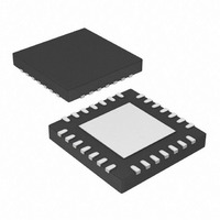
PIC16LF1827-I/MV Microchip Technology, PIC16LF1827-I/MV Datasheet - Page 15

PIC16LF1827-I/MV
Manufacturer Part Number
PIC16LF1827-I/MV
Description
IC, 8BIT MCU, PIC16LF, 32MHZ, QFN-28
Manufacturer
Microchip Technology
Series
PIC® XLP™ 16Fr
Specifications of PIC16LF1827-I/MV
Controller Family/series
PIC16LF
Eeprom Memory Size
256Byte
Ram Memory Size
384Byte
Cpu Speed
32MHz
No. Of Timers
5
Interface
EUSART, I2C, SPI
Core Size
8 Bit
Program Memory Size
4kWords
Core Processor
PIC
Speed
32MHz
Connectivity
I²C, SPI, UART/USART
Peripherals
Brown-out Detect/Reset, POR, PWM, WDT
Number Of I /o
16
Program Memory Type
FLASH
Eeprom Size
256 x 8
Ram Size
384 x 8
Voltage - Supply (vcc/vdd)
1.8 V ~ 3.6 V
Data Converters
A/D 12x10b
Oscillator Type
Internal
Operating Temperature
-40°C ~ 85°C
Package / Case
28-UFQFN Exposed Pad
Processor Series
PIC16LF
Core
PIC
Data Ram Size
256 B
Maximum Clock Frequency
32 KHz
Number Of Programmable I/os
16
Number Of Timers
5
Operating Supply Voltage
1.8 V to 3.6 V
Maximum Operating Temperature
+ 125 C
3rd Party Development Tools
52715-96, 52716-328, 52717-734
Development Tools By Supplier
PG164130, DV164035, DV244005, DV164005
Minimum Operating Temperature
- 40 C
On-chip Adc
10 bit, 12 Channel
On-chip Dac
5 bit
Lead Free Status / RoHS Status
Lead free / RoHS Compliant
Lead Free Status / RoHS Status
Lead free / RoHS Compliant
Available stocks
Company
Part Number
Manufacturer
Quantity
Price
- Current page: 15 of 406
- Download datasheet (4Mb)
TABLE 1-2:
2010 Microchip Technology Inc.
RB3/AN9/CPS9/MDOUT/
CCP1
RB4/AN8/CPS8/SCL1/SCK1/
MDCIN2
RB5/AN7/CPS7/P1B/TX
SCL2
RB6/AN5/CPS5/T1CKI/T1OSI/
P1C
ICSPCLK
RB7/AN6/CPS6/T1OSO/
P1D
ICSPDAT
Legend: AN = Analog input or output CMOS = CMOS compatible input or output
Note 1: Pin functions can be moved using the APFCON0 or APFCON1 register.
(1,3)
(1,3)
(2)
(1,3)
2: Functions are only available on the PIC16F/LF1827.
3: Default function location.
/SCK2
/CCP2
/P2B
/P1A
TTL = TTL compatible input
HV = High Voltage
(1,2,3)
Name
(2)
(1,3)
(1,2,3)
/SS1
/MDCIN1/
PIC16F/LF1826/27 PINOUT DESCRIPTION (CONTINUED)
/P2A
(1,3)
(1)
(1,2,3)
/CK
/
(1)
/
Function
ICSPCLK
ICSPDAT
MDCIN2
MDCIN1
MDOUT
T1OSO
T1OSO
T1CKI
CPS9
CCP1
CPS8
SCK1
CPS7
SCK2
CPS5
CCP2
CPS6
SCL1
SCL2
RB3
AN9
P1A
RB4
AN8
RB5
AN7
P1B
SS1
RB6
AN5
P1C
P2A
RB7
AN6
P1D
P2B
CK
TX
ST
XTAL = Crystal
Input
I
I
XTAL
XTAL
Type
= Schmitt Trigger input with CMOS levels I
2
2
TTL
TTL
TTL
TTL
TTL
AN
AN
AN
AN
AN
AN
AN
AN
AN
AN
ST
ST
ST
ST
ST
ST
ST
ST
ST
ST
ST
—
—
C™
—
—
C™
—
—
—
—
Output
Preliminary
CMOS General purpose I/O. Individually controlled interrupt-on-change.
CMOS Modulator output.
CMOS Capture/Compare/PWM1.
CMOS PWM output.
CMOS General purpose I/O. Individually controlled interrupt-on-change.
CMOS SPI clock 1.
CMOS General purpose I/O. Individually controlled interrupt-on-change.
CMOS PWM output.
CMOS USART asynchronous transmit.
CMOS USART synchronous clock.
CMOS SPI clock 2.
CMOS General purpose I/O. Individually controlled interrupt-on-change.
CMOS PWM output.
CMOS Capture/Compare/PWM2.
CMOS PWM output.
CMOS General purpose I/O. Individually controlled interrupt-on-change.
CMOS PWM output.
CMOS PWM output.
CMOS ICSP™ Data I/O.
XTAL
XTAL
Type
OD
OD
—
—
—
—
—
—
—
—
—
—
—
—
—
—
—
Individually enabled pull-up.
A/D Channel 9 input.
Capacitive sensing input 9.
Individually enabled pull-up.
A/D Channel 8 input.
Capacitive sensing input 8.
I
Modulator Carrier Input 2.
Individually enabled pull-up.
A/D Channel 7 input.
Capacitive sensing input 7.
I
Slave Select input 1.
Individually enabled pull-up.
A/D Channel 5 input.
Capacitive sensing input 5.
Timer1 clock input.
Timer1 oscillator connection.
Serial Programming Clock.
Individually enabled pull-up.
A/D Channel 6 input.
Capacitive sensing input 6.
Timer1 oscillator connection.
Modulator Carrier Input 1.
2
2
C™ clock 1.
C™ clock 2.
PIC16F/LF1826/27
Description
OD
2
C™ = Schmitt Trigger input with I
= Open Drain
levels
DS41391C-page 15
2
C
Related parts for PIC16LF1827-I/MV
Image
Part Number
Description
Manufacturer
Datasheet
Request
R

Part Number:
Description:
IC, 8BIT MCU, PIC16LF, 32MHZ, QFN-28
Manufacturer:
Microchip Technology
Datasheet:

Part Number:
Description:
IC, 8BIT MCU, PIC16LF, 32MHZ, DIP-18
Manufacturer:
Microchip Technology
Datasheet:

Part Number:
Description:
IC, 8BIT MCU, PIC16LF, 20MHZ, TQFP-44
Manufacturer:
Microchip Technology
Datasheet:

Part Number:
Description:
7 KB Flash, 384 Bytes RAM, 32 MHz Int. Osc, 16 I/0, Enhanced Mid Range Core, Nan
Manufacturer:
Microchip Technology

Part Number:
Description:
14KB Flash, 512B RAM, LCD, 11x10b ADC, EUSART, NanoWatt XLP 28 SOIC .300in T/R
Manufacturer:
Microchip Technology
Datasheet:

Part Number:
Description:
14KB Flash, 512B RAM, LCD, 11x10b ADC, EUSART, NanoWatt XLP 28 SSOP .209in T/R
Manufacturer:
Microchip Technology
Datasheet:

Part Number:
Description:
MCU PIC 14KB FLASH XLP 28-SSOP
Manufacturer:
Microchip Technology

Part Number:
Description:
MCU PIC 14KB FLASH XLP 28-SOIC
Manufacturer:
Microchip Technology

Part Number:
Description:
MCU PIC 512B FLASH XLP 28-UQFN
Manufacturer:
Microchip Technology

Part Number:
Description:
MCU PIC 14KB FLASH XLP 28-SPDIP
Manufacturer:
Microchip Technology

Part Number:
Description:
MCU 7KB FLASH 256B RAM 40-UQFN
Manufacturer:
Microchip Technology

Part Number:
Description:
MCU 7KB FLASH 256B RAM 44-TQFP
Manufacturer:
Microchip Technology

Part Number:
Description:
MCU 14KB FLASH 1KB RAM 28-UQFN
Manufacturer:
Microchip Technology

Part Number:
Description:
MCU PIC 14KB FLASH XLP 40-UQFN
Manufacturer:
Microchip Technology

Part Number:
Description:
MCU PIC 14KB FLASH XLP 44-TQFP
Manufacturer:
Microchip Technology


