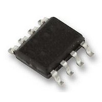
LP2996M National Semiconductor, LP2996M Datasheet - Page 13

LP2996M
Manufacturer Part Number
LP2996M
Description
IC, REG DDR TERMINATION, SMD, SO-8
Manufacturer
National Semiconductor
Datasheet
1.LP2996M.pdf
(18 pages)
Specifications of LP2996M
Primary Input Voltage
2.5V
Output Voltage
1.35V
No. Of Pins
8
Output Current
1.5A
Voltage Regulator Case Style
SOIC
Operating Temperature Range
0°C To +125°C
Svhc
No SVHC (15-Dec-2010)
Output Voltage Fixed
1.35V
Rohs Compliant
Yes
Lead Free Status / RoHS Status
Lead free / RoHS Compliant
Available stocks
Company
Part Number
Manufacturer
Quantity
Price
Company:
Part Number:
LP2996M
Manufacturer:
nstion
Quantity:
217
Company:
Part Number:
LP2996MMX
Manufacturer:
AGILENT
Quantity:
700
Part Number:
LP2996MMX
Manufacturer:
NS/国半
Quantity:
20 000
Company:
Part Number:
LP2996MR
Manufacturer:
ns
Quantity:
2 560
Part Number:
LP2996MR
Manufacturer:
NS/国半
Quantity:
20 000
Company:
Part Number:
LP2996MR/NOPB
Manufacturer:
SANYO
Quantity:
195
Part Number:
LP2996MR/NOPB
Manufacturer:
NS/国半
Quantity:
20 000
Company:
Part Number:
LP2996MRX
Manufacturer:
TI
Quantity:
6 222
Part Number:
LP2996MRX
Manufacturer:
NS/国半
Quantity:
20 000
Part Number:
LP2996MRX/NOPB
Manufacturer:
TI/德州仪器
Quantity:
20 000
LEVEL SHIFTING
If standards other than SSTL-2 are required, such as SSTL-3,
it may be necessary to use a different scaling factor than 0.5
times V
are available to scale the output to any voltage required. One
method is to level shift the output by using feedback resistors
Conversely, the R2 resistor can be placed between V
and V
ence voltage of VDDQ/2. The equations relating VTT and the
resistors can be seen below:
HSTL APPLICATIONS
The LP2996 can be easily adapted for HSTL applications by
connecting V
DDQ
DDQ
to shift the V
for regulating the output voltage. Several options
DDQ
to the 1.5V rail. This will produce a V
TT
output lower than the internal refer-
FIGURE 11. Decreasing VTT by Level Shifting
FIGURE 10. Increasing VTT by Level Shifting
FIGURE 12. HSTL Application
TT
SENSE
and
13
from V
10 and 11. Figure 10 shows how to use two resistors to level
shift V
calculate the exact voltage at V
be used.
V
sistors. AVIN and PVIN should be connected to a 2.5V rail for
optimal performance.
REF
voltage of approximately 0.75V for the termination re-
TT
TT
to the V
above the internal reference voltage of VDDQ/2. To
SENSE
V
V
TT
TT
= VDDQ/2 ( 1 + R1/R2)
= VDDQ/2 (1 - R1/R2)
20057516
pin. This has been illustrated in Figures
20057515
20057517
TT
the following equation can
www.national.com


