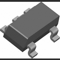
SI91841DT-25-T1 Vishay, SI91841DT-25-T1 Datasheet

SI91841DT-25-T1
Specifications of SI91841DT-25-T1
Available stocks
Related parts for SI91841DT-25-T1
SI91841DT-25-T1 Summary of contents
Page 1
... The Si91841 features reverse battery protection to limit reverse current flow to approximately 1-mA in the event reversed battery is applied at the input, thus preventing damage to the IC. The Si91841 is available in both standard and lead (Pb)-free packages. Si91841 OUT GND Thin SOT-23, 5-Lead Si91841 Vishay Siliconix V OUT www.vishay.com 1 ...
Page 2
... Si91841 Vishay Siliconix ABSOLUTE MAXIMUM RATINGS Absolute Maximum Ratings Input Voltage GND . . . . . . . . . . . . . . . . . . . . . . . . . . . . . . . . . . . . . . IN V (See Detailed Description Output Current OUT Output Voltage OUT b Package Power Dissipation Stresses beyond those listed under “Absolute Maximum Ratings” may cause permanent damage to the device. These are stress ratings only, and functional operation of the device at these or any other conditions beyond those indicated in the operational sections of the specifications is not implied ...
Page 3
... (See Figure 1 100 nA SD LOAD < are measured 1.8 V. OUT OUT IN 0.95 V NOM V OUT FIGURE 1. Timing Diagram for Power-Up Si91841 Vishay Siliconix Limits −40 to 85_C Min Typ Max Unit a a Temp Temp Room 30 mV(rms) Room 60 Room 40 Room 30 Room 20 Room 20 Room 150 ...
Page 4
... Pin No OUT GND Lead (Pb)-Free Part Number Part Number Si91841DT-18-T1 Si91841DT-18-T1—E3 Si91841DT-25-T1 Si91841DT-25-T1—E3 Si91841DT-26-T1 Si91841DT-26-T1—E3 Si91841DT-28-T1 Si91841DT-28-T1—E3 Si91841DT-285-T1 Si91841DT-285—E3 Si91841DT-29-T1 Si91841DT-29-T1—E3 Si91841DT-30-T1 Si91841DT-30-T1—E3 Si91841DT-33-T1 Si91841DT-33-T1—E3 Si91841DT-50-T1 Si91841DT-50-T1—E3 Note Lot Code www.vishay.com 4 Name ...
Page 5
... Si91841 Vishay Siliconix Normalized V vs. Temperature OUT 0 OUT(nom) 0 OUT I OUT I = 150 mA OUT −40 − Ambient Temperature (_C) No Load GND Pin Current vs. Input Voltage ...
Page 6
... Si91841 Vishay Siliconix TYPICAL CHARACTERISTICS (INTERNALLY REGULATED, 25_C UNLESS NOTED) Dropout Voltage vs. Load Current 350 V = 3.0 V OUT 300 250 200 150 100 120 180 I LOAD (mA) Dropout Voltage vs. Temperature 350 V = 3.0 V OUT 300 I = 300 mA OUT 250 200 I = 150 mA 150 OUT 100 OUT ...
Page 7
... LineTransient Response-1 V OUT 10 mV/div V/div 20 ms/div INSTEP OUT OUT 150 mA LOAD msec rise Document Number: 71447 S-50956—Rev. D, 16-May-05 Vishay Siliconix Load Transient Response-2 V OUT 10 mV/div I LOAD 100 mA/div 20 ms/div V = 3.0 V OUT OUT I = 150 LOAD msec fall LineTransient Respons-2 V OUT 10 mV/div V/div ...
Page 8
... Si91841 Vishay Siliconix TYPICAL WAVEFORMS Output Noise V OUT 200 mV/div 4 ms/div OUT I = 150 mA OUT C = 0.01 mF NOISE 100 kHz BLOCK DIAGRAM Reverse Polarity V IN Protection Reference Shutdown SD Control www.vishay.com 0.01 Si91841 − + Thermal Sensor Current Limit Noise Spectrum OUT I = 150 mA LOAD C = 0.01 mF ...
Page 9
... IN the SD pin to V via a 100-kW resistor if reverse battery IN Vishay Siliconix maintains worldwide manufacturing capability. Products may be manufactured at one of several qualified locations. Reliability data for Silicon Technology and Package Reliability represent a composite of all qualified locations. http://www.vishay.com/ppg?71447. Document Number: 71447 S-50956—Rev. D, 16-May-05 protection is desired ...
Page 10
... Vishay disclaims any and all liability arising out of the use or application of any product described herein or of any information provided herein to the maximum extent permitted by law. The product specifications do not expand or otherwise modify Vishay’ ...


