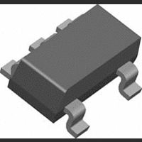
SI91841DT-25-T1 Vishay, SI91841DT-25-T1 Datasheet - Page 9

SI91841DT-25-T1
Manufacturer Part Number
SI91841DT-25-T1
Description
IC, LDO VOLT REG, 2.5V, 150mA, 5-SOT-23
Manufacturer
Vishay
Datasheet
1.SI91841DT-18-T1.pdf
(10 pages)
Specifications of SI91841DT-25-T1
Primary Input Voltage
6V
Output Voltage Fixed
2.5V
Dropout Voltage Vdo
190mV
No. Of Pins
5
Output Current
150mA
Operating Temperature Range
-40°C To +85°C
Termination Type
SMD
Lead Free Status / RoHS Status
Contains lead / RoHS non-compliant
Available stocks
Company
Part Number
Manufacturer
Quantity
Price
Company:
Part Number:
SI91841DT-25-T1
Manufacturer:
Vishay
Quantity:
16 950
Company:
Part Number:
SI91841DT-25-T1
Manufacturer:
MOLEX
Quantity:
20 562
Part Number:
SI91841DT-25-T1
Manufacturer:
VISHAY/威世
Quantity:
20 000
Company:
Part Number:
SI91841DT-25-T1-E3
Manufacturer:
Vishay
Quantity:
16 950
Part Number:
SI91841DT-25-T1-E3
Manufacturer:
VISHAY/威世
Quantity:
20 000
DETAILED DESCRIPTION
The Si91841 is a low-noise, low drop-out and low quiescent
current linear voltage regulator, packaged in a small footprint
Thin SOT23-5 package. The Si91841 can supply loads up to
150 mA. As shown in the block diagram, the circuit consists of
a bandgap reference error, amplifier, p-channel pass transistor
and feedback resistor string. An external bypass capacitor
connected to the BP pin reduces noise at the output.
Additional blocks, not shown in the block diagram, include a
precise current limiter, reverse battery and current protection
and thermal sensor.
Thermal Overload Protection
The thermal overload protection limits the total power
dissipation and protects the device from being damaged.
When the junction temperature exceeds 150_, the device
turns the p-channel pass transistor off.
Reverse Battery Protection
The Si91841 has a battery reverse protection circuitry that
disconnects the internal circuitry when V
GND voltage. There is no current drawn in such an event.
When the SD pin is hardwired to V
the SD pin to V
Vishay Siliconix maintains worldwide manufacturing capability. Products may be manufactured at one of several qualified locations. Reliability data for Silicon Technology and
Package Reliability represent a composite of all qualified locations.
http://www.vishay.com/ppg?71447.
Document Number: 71447
S-50956—Rev. D, 16-May-05
IN
via a 100-kW resistor if reverse battery
IN
, the user must connect
IN
drops below the
For related documents such as package/tape drawings, part marking, and reliability data, see
protection is desired. Hardwiring the SD pin directly to the V
pin is allowed when reverse battery protection is not desired.
Noise Reduction
An external 10-nF bypass capacitor at BP is used to create a
low pass filter for noise reduction. The start-up time is fast,
since a power-on circuit pre-charges the bypass capacitor.
After the power-up sequence the pre-charge circuit is switched
to standby mode in order to save current. It is therefore not
recommended to use larger bypass capacitor values than
50 nF. When the circuit is used without a capacitor, stable
operation is guaranteed.
Auto-Discharge/No-Discharge
For Si91841 only, V
path to ground when the SD pin is low.
Stability
The circuit is stable with only a small output capacitor equal to
6 nF/mA (= 1 mF @ 150 mA). Since the bandwidth of the error
amplifier is around 1−3 MHz and the dominant pole is at the
output node, the capacitor should be capacitive in this range,
i.e., for 150-mA load current, an ESR <0.4 W is necessary.
Parasitic inductance of about 10 nH can be tolerated.
OUT
has an internal 100-W (typ.) discharge
Vishay Siliconix
Si91841
www.vishay.com
IN
9


