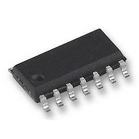
UCC35701D UNITRODE, UCC35701D Datasheet - Page 6

UCC35701D
Manufacturer Part Number
UCC35701D
Description
PWM CONTROLLER, SMD, 35701, SOIC14
Manufacturer
UNITRODE
Datasheet
1.UCC35701D.pdf
(23 pages)
Specifications of UCC35701D
Input Voltage
11V
Output Voltage
1V
Output Current
100mA
Frequency
700kHz
Supply Voltage Range
10V To 13V
Digital Ic Case Style
SOIC
No. Of Pins
14
Operating Temperature Range
0°C To +70°C
Available stocks
Company
Part Number
Manufacturer
Quantity
Price
Company:
Part Number:
UCC35701D
Manufacturer:
SIPEX
Quantity:
6 781
Part Number:
UCC35701D
Manufacturer:
UC
Quantity:
20 000
APPLICATION INFORMATION (cont.)
Output Inhibit
During normal operation, OUT is driven high at the start
of a clock period and is driven low by voltages on CT, FB
or VSCLAMP.
The following conditions cause the output to be immedi-
ately driven low until a clock period starts where none of
the conditions are true:
1. I
2. FB or SS is less than 0.8V
Current Limiting
ILIM is monitored by two internal comparators. The cur-
rent limit comparator threshold is 0.2V. If the current limit
comparator is triggered, OUT is immediately driven low
and held low for the remainder of the clock cycle, provid-
ing pulse-by-pulse over-current control for excessive
loads. This comparator also causes C
the remainder of the clock cycle.
If repetitive cycles are terminated by the current limit
comparator causing COUNT to rise above 4V, the shut-
down latch is set. The COUNT integration delay feature
will be bypassed by the shutdown comparator which has
a 0.6V threshold. The shutdown comparator immediately
sets the shutdown latch. R
COUNT integrator following transient faults. R
greater than (4 · R4) · (1 – D
Latched Shutdown
If ILIM rises above 0.6V, or COUNT rises to 4V, the shut-
down latch will be set. This will force OUT low, discharge
SS and COUNT, and reduce I
750mA. When, and if, V
threshold, the shutdown latch will reset and I
to 130mA, allowing the circuit to restart. If V
above the UVLO stop threshold (within the UVLO band),
an alternate restart will occur if VFF is momentarily re-
duced below 1V. External shutdown commands from any
source may be added into either the COUNT or ILIM
pins.
Voltage Feedforward
The voltage slope on CT is proportional to line voltage
over a 4:1 range and equals 2·VFF (RT·CT). The capac-
itor charging current is set by the voltage across R
V(RT) tracks VFF over a range of 0.8V to 3.2V. A chang-
ing line voltage will immediately change the slope of
V(CT), changing the pulse width in a proportional manner
without using the feedback loop, providing excellent dy-
namic line regulation.
LIM
> 0.2V
DD
F
in parallel with C
MAX
falls below the UVLO stop
).
DD
F
to approximately
to be charged for
F
DD
DD
F
resets the
must be
remains
will fall
T
.
6
VFF is intended to operate accurately over a 4:1 range
between 0.8V and 3.2V. Voltages at VFF below 0.6V or
above 4.0V will initiate a soft stop cycle and a chip restart
when the under/over voltage condition is removed.
Volt-Second Clamp
A constant volt-second clamp is formed by comparing the
timing capacitor ramp voltage to a fixed voltage derived
from the reference. Resistors R4 and R5 set the
volt-second limit. For a volt-second product defined as
VIN t
The duty cycle limit is then:
The maximum duty cycle is realized when the
feedforward voltage is set at the low end of the operating
range (V
The absolute maximum duty cycle is:
Frequency Set
The frequency is set by a resistor from RT to ground and
a capacitor from CT to ground. The frequency is approxi-
mately: F
External synchronization is via the SYNC pin. The pin
has a 1.5V threshold , making it compatible with 5V and
3.3V CMOS logic. The input is level sensitive, with a high
input forcing the oscillator ramp low and the output low.
An active pull down on the SYNC pin allows it to be un-
connected when not used.
Gate Drive Output
The UCC35701/2 is capable of a 1A peak output current.
Bypass with at least 0.1mF directly to PGND. The capac-
itor must have a low equivalent series resistance and in-
ductance. The connection from OUT to the power
MOSFET gate should have a 2W or greater damping re-
sistor and the distance between chip and MOSFET
should be minimized. A low impedance path must be es-
tablished between the MOSFET source (or ground side
of the current sense resistor), the V
PGND. PGND should then be connected by a single path
(shown as RGND) to GND.
V
D
æ
ç
è
VS CLAMP
R
MAX
V
1
ON(max)
R
VFF
+
FF
2
R
=
=
2
= 0.8V).
V
(
ö
÷ ·
ø
VS CLAMP
R
, or
R
, the required voltage at VSCLAMP is:
T
T
0 8
(
V
·
.
2
·
IN
C
V
C
T
IN
T
·
V
)
t
VS CLAMP
·
=
ON
æ
ç
è
V
R
(
0 8
R EF
ma x
1
.
R
+
2
)
R
·
)
2
R
.
ö
÷
ø
.
4
R
+
5
R
5
DD
UCC15701/2
UCC25701/2
UCC35701/2
capacitor and


