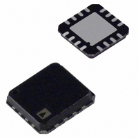
AD8352ACPZ-R7 Analog Devices Inc, AD8352ACPZ-R7 Datasheet

AD8352ACPZ-R7
Specifications of AD8352ACPZ-R7
Related parts for AD8352ACPZ-R7
AD8352ACPZ-R7 Summary of contents
Page 1
FEATURES −3 dB bandwidth of 2.2 GHz ( dB) V Single resistor gain adjust ≤ A ≤ Single resistor and capacitor distortion adjust Input resistance: 3 kΩ, independent of gain (A Differential or ...
Page 2
AD8352 TABLE OF CONTENTS Features .............................................................................................. 1 Applications ....................................................................................... 1 Functional Block Diagram .............................................................. 1 General Description ......................................................................... 1 Revision History ............................................................................... 2 Specifications ..................................................................................... 3 Noise Distortion Specifications .................................................. 4 Absolute Maximum Ratings ............................................................ 6 ESD Caution .................................................................................. 6 ...
Page 3
SPECIFICATIONS 200 Ω differential 118 Ω otherwise noted. C and R are selected for differential broadband operation (see Table 5 and Table 6 Table 1. Parameter ...
Page 4
AD8352 NOISE DISTORTION SPECIFICATIONS 200 Ω differential 118 Ω otherwise noted. C and R are selected for differential broadband operation (see Table 5 and Table 6). See the ...
Page 5
Parameter 190 MHz Second/Third Harmonic Distortion Output Third-Order Intercept Third-Order IMD Noise Spectral Density (RTI Compression Point (RTO) 240 MHz Second/Third Harmonic Distortion Output Third-Order Intercept Third-Order IMD Noise Spectral Density (RTI Compression Point (RTO) 380 ...
Page 6
AD8352 ABSOLUTE MAXIMUM RATINGS Table 3. Parameter Supply Voltage, VCC VIP, VIN Internal Power Dissipation θ JA Maximum Junction Temperature Operating Temperature Range Storage Temperature Range Lead Temperature (Soldering 60 sec) Stresses above those listed under Absolute Maximum Ratings may ...
Page 7
PIN CONFIGURATION AND FUNCTION DESCRIPTIONS Table 4. Pin Function Descriptions Pin No. Mnemonic Description 1 RDP Positive Distortion Adjust. 2 RGP Positive Gain Adjust. 3 RGN Negative Gain Adjust. 4 RDN Negative Distortion Adjust. 5 VIN Balanced Differential Input. This ...
Page 8
AD8352 TYPICAL PERFORMANCE CHARACTERISTICS 43Ω 100Ω 520Ω –5 10 100 FREQUENCY (MHz) Figure 4. Gain vs. Frequency for a 200 Ω Differential Load with Baluns, ...
Page 9
OIP3 10dB 6dB 10dB 10dB V NOISE FIGURE 100 150 200 250 300 350 FREQUENCY (MHz) Figure 10. ...
Page 10
AD8352 0.6 0.5 0.4 0.3 0.2 0 100 200 300 400 500 600 FREQUENCY (MHz) Figure 16. Group Delay and Phase vs. Frequency, A 3500 3000 2500 2000 1500 1000 500 0 0 100 200 300 400 500 ...
Page 11
APPLICATIONS INFORMATION GAIN AND DISTORTION ADJUSTMENT (DIFFERENTIAL INPUT) Table 5 and Table 6 show the required value of R specified at 200 Ω and 1 kΩ loads. Figure 22 and Figure 24 plot gain vs ...
Page 12
AD8352 100 200 300 400 500 R (Ω) G Figure 24. Gain vs ...
Page 13
This broadband optimization was also performed at 180 MHz. As with differential input drive, the resulting distortion levels at lower frequencies are based on the C D Table 7 and Table 8. As with differential input drive, relative third-order reduction ...
Page 14
AD8352 6dB V 43 10dB 15dB 42 18dB 100 FREQUENCY (MHz) Figure 32. Third-Order Intermodulation Distortion, OIP3 vs. Frequency for Various Gain Settings 6.0 5.5 5.0 4.5 ...
Page 15
V CC 0.1µF 0Ω IF/RF INPUT 2 AD8352 R R 50Ω ADT1-1WT 0Ω 0.1µF 0.1µF Figure 34. Differential Input to the AD8352 Driving the 0.1µF VIP VOP 50Ω ...
Page 16
AD8352 EVALUATION BOARD An evaluation board is available for experimentation of various parameters such as gain, common-mode level, and distortion. The output network can be configured for different loads via minor output component changes. The schematic and evaluation board artwork ...
Page 17
EVALUATION BOARD SCHEMATICS VCC VCC VCM GND ENB GND Figure 38. AD8352 Evaluation Board, Version A01212A Rev Page AD8352 05728-017 ...
Page 18
AD8352 Figure 40. Far Side Showing Ground Plane Pull Back Around Critical Features Figure 39. Component Side Silkscreen Rev Page ...
Page 19
... OUTLINE DIMENSIONS PIN 1 INDICATOR 12° MAX 0.90 0.85 0.80 SEATING PLANE ORDERING GUIDE Model Temperature Range 1 AD8352ACPZ-WP −40°C to +85°C 1 AD8352ACPZ-R7 −40°C to +85°C 1 AD8352ACPZ-R2 −40°C to +85°C 1 AD8352-EVALZ RoHS Compliant Part. 3.00 0.60 MAX BSC SQ 0. 2.75 ...
Page 20
AD8352 NOTES ©2006–2008 Analog Devices, Inc. All rights reserved. Trademarks and registered trademarks are the property of their respective owners. D05728-0-7/08(B) Rev Page ...


