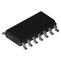
HFA3600IB Intersil, HFA3600IB Datasheet - Page 13

HFA3600IB
Manufacturer Part Number
HFA3600IB
Description
IC, LOW-NOISE AMP, 19.8DB 900MHZ SOIC-14
Manufacturer
Intersil
Datasheet
1.HFA3600IB.pdf
(16 pages)
Specifications of HFA3600IB
Frequency Range
900MHz
Noise Figure Typ
3.97dB
Power Dissipation Pd
1W
Supply Current
11.3mA
Supply Voltage Range
4V To 5.5V
Gain
19.8dB
Rf Type
Cellular, GSM, ISM, PCS
Lead Free Status / RoHS Status
Contains lead / RoHS non-compliant
optimum performance and tight distribution among production
lots. The open collector output permits direct interface to
moderate impedance IF filters as well as 50W input filters after
a simple “L” impedance matching network. A collector resistor
of 1K has been used throughout the characterization together
with an impedance matching network for 50W load
measurements. With a low -3dBm LO level, a typical SSB noise
figure of 12.1dB, conversion gain of 7.0dB and a third order
output intercept point of +3.2dBm are the main features. The
LO input return loss is typically of 26dBm and the RF input
return loss has a typical value of 11dB.
Bias Network and Power Down
The Bias Network is responsible for the accurate setting of
both LNA and MIXER operating currents. The LNA operating
current is accurately set to 5mA while the MIXER is set to
4mA. Laser trimming procedures and a temperature
independent performance of the bias cell, assure the worst
case operating current variation of the LNA and MIXER of
1% over the operating temperature range.
The Bias network is powered by the Mixer V
a built in feature of disabling both the LNA and the MIXER
stages. The cell can be powered up and down within 10ms.
Power down total current consumption is in the order of
250mA. The simplified schematic of the power down input
circuit is shown below.
Low Voltage Operation
Low voltage operation is possible with the HFA3600. The
HFA3600 has been characterized with V
moderate degradations have been observed compared to
the AC performance at a V
0.8dB decrease and a 1.5dB degradation in the output
intercept point with no measurable impact on noise figure.
The MIXER behavior at 4V can be summarized with a
degradation of conversion gain and output intercept point of
0.8dB and a slight improvement in noise figure of 0.6dB.
PD
FIGURE 35. ENABLE PIN INPUT CIRCUIT
15K
CC
100K
13
of 5V. The LNA gain shows a
CC
10K
of 4V and only
CC
MIXER V
pin and has
CC
HFA3600
Other relevant 4V performance characteristics include:
Layout Considerations
The HFA3600 evaluation board layout has been carefully
designed for an accurate RF characterization of the device.
50 microstrip lines have been provided to permit the
connection of the LNA and MIXER independently and
facilitate the user interface for testing. Top ground planes
were used to assure adequate isolation between critical
traces.
The HA3600 package pinout has been laid out for best
isolation and overall device performance which also permits
the placement and connection of ground planes at pins 2, 4,
5, 10 and 12. Pin 4 and Pin 5 assure a low impedance
ground return for the LNA and also helps the isolation
between the LNA input and the LO input. The LNA output pin
is isolated from the RF input port with a good ground
connection between the top and back ground planes
terminated at pin 10. A series of plated through holes
resembling a stitch pattern are sufficient and important for
the LNA
rely on the full characteristics of rejection of the image filter.
Similar isolation pattern is drawn and terminated in pin 12 to
isolate the RF
A ground pad has been laid down beneath the package with a
series of plated through holes to minimize the inductance to
the ground plane and improve the device gain characteristics.
All device grounds must be connected as close to the
package as possible and the same applies to both V
inputs and all V
tantalum capacitor at the V
coupling to the bias network if the device is subjected to
strong low frequency interference signals.
A protection diode has been added to the demonstration
board for extra protection and is not needed in an actual
application.
• Total ICC: typical drop of 2.2mA
• LNA Input Return Loss: degraded by 0.6dB
• LNA Reverse Isolation: degraded by 1dB
• LNA Output Return Loss: degraded by 1dB
• RF to IF Isolation: no change
• LOin to LNAin Isolation: improvement by 2dB
• LNAOUT to Mixer RFIN Isolation: improvement by
• Mixer LO to RF Isolation: no change
• Mixer LO to IF Isolation: degrades by 0.5dB
• Mixer RF input Return Loss: degrades by 1dB
• Mixer LO Input Return Loss: degrades by 0.3dB at
0.2dB
800MHz and 1dB at 700MHz
-OUT
and RF
-IN
CC
from the IF
bypass capacitors. A small 4.7 F
-IN
ports isolation, so the designer can
CC
-OUT
line will prevent supply
port.
CC


