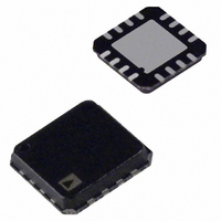
ADG1636BCPZ-REEL7 Analog Devices Inc, ADG1636BCPZ-REEL7 Datasheet - Page 3

ADG1636BCPZ-REEL7
Manufacturer Part Number
ADG1636BCPZ-REEL7
Description
IC, ANALOG SWITCH, DUAL, SPDT, LFCSP-16
Manufacturer
Analog Devices Inc
Type
Analog Switchr
Datasheet
1.ADG1636BRUZ.pdf
(16 pages)
Specifications of ADG1636BCPZ-REEL7
Analog Switch Type
SPDT
No. Of Channels
2
Bandwidth
25MHz
On State Resistance Max
1ohm
Turn Off Time
182ns
Turn On Time
119ns
Supply Voltage Range
3.3V To 16V
Design Resources
Precision Pulse Oximeter LED Current Sinks Using ADA4505-2, ADR1581, and ADG1636 (CN0125)
Function
Switch
Circuit
2 x SPDT
On-state Resistance
1.2 Ohm
Voltage Supply Source
Single, Dual Supply
Voltage - Supply, Single/dual (±)
3.3 V ~ 16 V, ±3.3 V ~ 8 V
Current - Supply
1µA
Operating Temperature
-40°C ~ 85°C
Mounting Type
Surface Mount
Package / Case
16-VQFN, CSP Exposed Pad
Rohs Compliant
Yes
Multiplexer Configuration
Dual SPDT
Number Of Inputs
2
Number Of Outputs
4
Number Of Channels
2
Power Supply Requirement
Single/Dual
Single Supply Voltage (min)
3.3V
Single Supply Voltage (typ)
5/9/12/15V
Single Supply Voltage (max)
16V
Dual Supply Voltage (typ)
±5V
Dual Supply Voltage (max)
±8V
Mounting
Surface Mount
Pin Count
16
Operating Temp Range
-40C to 125C
Operating Temperature Classification
Automotive
Lead Free Status / RoHS Status
Lead free / RoHS Compliant
Lead Free Status / RoHS Status
Lead free / RoHS Compliant, Lead free / RoHS Compliant
Other names
ADG1636BCPZ-REEL7TR
Available stocks
Company
Part Number
Manufacturer
Quantity
Price
Company:
Part Number:
ADG1636BCPZ-REEL7
Manufacturer:
ADI
Quantity:
3 391
SPECIFICATIONS
±5 V DUAL SUPPLY
V
Table 1.
Parameter
ANALOG SWITCH
LEAKAGE CURRENTS
DIGITAL INPUTS
DYNAMIC CHARACTERISTICS
POWER REQUIREMENTS
1
Guaranteed by design, not subject to production test.
DD
Analog Signal Range
On Resistance (R
On Resistance Match Between Channels (∆R
On Resistance Flatness (R
Source Off Leakage, I
Drain Off Leakage, I
Channel On Leakage, I
Input High Voltage, V
Input Low Voltage, V
Input Current, I
Digital Input Capacitance, C
Transition Time, t
t
t
Break-Before-Make Time Delay, t
Charge Injection
Off Isolation
Channel-to-Channel Crosstalk
Total Harmonic Distortion + Noise (THD + N)
−3 dB Bandwidth
C
C
C
I
V
DD
ON
OFF
DD
S
D
D
= +5 V ± 10%, V
, C
(Off )
(Off )
(EN)
/V
(EN)
S
SS
(On)
INL
ON
TRANSITION
or I
)
SS
D
INL
INH
S
(Off )
= −5 V ± 10%, GND = 0 V, unless otherwise noted.
INH
(Off )
D
, I
S
FLAT(ON)
(On)
1
IN
)
D
ON
)
25°C
1
1.2
0.04
0.08
0.2
0.25
±0.1
±0.25
±0.1
±0.25
±0.3
±0.6
0.005
5
130
209
119
148
182
228
30
130
70
90
0.007
25
68
127
220
0.001
−40°C to
+85°C
1.4
0.09
0.29
±1
±2
±2
245
166
259
Rev. A | Page 3 of 16
−40°C to
+125°C
V
1.6
0.1
0.34
±4
±10
±12
2.0
0.8
±0.1
273
176
281
17
1.0
±3.3/±8
DD
to V
SS
ns max
ns max
ns typ
ns max
Unit
V
Ω typ
Ω max
Ω typ
Ω max
Ω typ
Ω max
nA typ
nA max
nA typ
nA max
nA typ
nA max
V min
V max
μA typ
μA max
pF typ
ns typ
ns typ
ns typ
ns min
pC typ
dB typ
dB typ
% typ
MHz typ
pF typ
pF typ
pF typ
μA typ
μA max
V min/max
Test Conditions/Comments
V
V
V
V
V
V
V
V
V
R
V
R
V
R
V
R
V
V
R
R
R
see Figure 29
R
V
V
V
V
Digital inputs = 0 V or V
L
L
L
L
L
L
L
L
S
DD
S
S
DD
S
S
S
IN
S
S
S
S1
S
S
S
S
DD
= 50 Ω, C
= 50 Ω, C
= ±4.5 V, I
= ±4.5 V, I
= ±4.5 V, I
= ±4.5 V, V
= ±4.5V, V
= V
= 300 Ω, C
= 2.5 V; see Figure 30
= 300 Ω, C
= 2.5 V; see Figure 30
= 300 Ω, C
= 2.5 V; see Figure 30
= 300 Ω, C
= 0 V, R
= 110 Ω, 5 V p-p, f = 20 Hz to 20 kHz;
= 50 Ω, C
= 0 V, f = 1 MHz
= 0 V, f = 1 MHz
= 0 V, f = 1 MHz
= V
= V
= ±4.5 V, V
= +5.5 V, V
= +5.5 V, V
D
GND
S2
= ±4.5 V; see Figure 25
= 2.5 V; see Figure 31
S
or V
= 0 Ω, C
L
L
L
= 5 pF, f = 1 MHz; see Figure 26
= 5 pF, f = 1 MHz; see Figure 28
S
S
S
D
= 5 pF; see Figure 27
D
L
L
L
L
= −10 mA; see Figure 23
= −10 mA
= −10 mA
DD
= ∓4.5 V; see Figure 24
= 35 pF
= 35 pF
= 35 pF
= 35 pF
SS
SS
SS
= ∓4.5 V; see Figure 24
= ±4.5 V
= −5.5 V
= −5.5 V
L
= 1 nF; see Figure 32
DD
ADG1636


