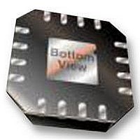
ADP2107ACPZ-1.8 Analog Devices Inc, ADP2107ACPZ-1.8 Datasheet - Page 15

ADP2107ACPZ-1.8
Manufacturer Part Number
ADP2107ACPZ-1.8
Description
V REG, 2A 1.8V, SMD, LFCSP-16, 2107
Manufacturer
Analog Devices Inc
Datasheet
1.ADP2105ACPZ-1.8-R7.pdf
(36 pages)
Specifications of ADP2107ACPZ-1.8
Primary Input Voltage
3.6V
No. Of Outputs
1
Output Voltage
1.8V
Output Current
2A
Voltage Regulator Case Style
LFCSP
No. Of Pins
16
Operating Temperature Range
-40°C To +125°C
Svhc
No SVHC
Lead Free Status / RoHS Status
Lead free / RoHS Compliant
SLOPE COMPENSATION
Slope compensation stabilizes the internal current control loop
of the ADP2105/ADP2106/ADP2107 when operating beyond
50% duty cycle to prevent subharmonic oscillations. It is imple-
mented by summing a fixed, scaled voltage ramp to the current
sense signal during the on-time of the P-channel MOSFET switch.
The slope compensation ramp value determines the minimum
inductor that can be used to prevent subharmonic oscillations
at a given output voltage. For slope compensation ramp values,
see Table 5. For more information see the Inductor Selection
section.
Table 5. Slope Compensation Ramp Values
Part
ADP2105
ADP2106
ADP2107
DESIGN FEATURES
Enable/Shutdown
Drive EN high to turn on the ADP2105/ADP2106/ADP2107.
Drive EN low to turn off the ADP2105/ADP2106/ADP2107,
reducing the input current below 0.1 μA. To force the
ADP2105/ADP2106/ADP2107 to automatically start when
input power is applied, connect EN to IN. When shut down, the
ADP2105/ADP2106/ADP2107 discharge the soft start capacitor,
causing a new soft start cycle every time they are re-enabled.
Synchronous Rectification
In addition to the P-channel MOSFET switch, the ADP2105/
ADP2106/ADP2107 include an integrated N-channel MOSFET
synchronous rectifier. The synchronous rectifier improves effi-
ciency, especially at low output voltage, and reduces cost and
board space by eliminating the need for an external rectifier.
Current Limit
The ADP2105/ADP2106/ADP2107 have protection circuitry to
limit the direction and amount of current flowing through the
power switch and synchronous rectifier. The positive current
limit on the power switch limits the amount of current that can
flow from the input to the output, and the negative current limit
on the synchronous rectifier prevents the inductor current from
reversing direction and flowing out of the load.
Slope Compensation Ramp Values
0.72 A/μs
1.07 A/μs
1.38 A/μs
Rev. C | Page 15 of 36
Short-Circuit Protection
The ADP2105/ADP2106/ADP2107 include frequency foldback
to prevent output current runaway on a hard short. When the
voltage at the feedback pin falls below 0.3 V, indicating the possi-
bility of a hard short at the output, the switching frequency is
reduced to 1/4 of the internal oscillator frequency. The reduction
in the switching frequency results in more time for the inductor to
discharge, preventing a runaway of output current.
Undervoltage Lockout (UVLO)
To protect against deep battery discharge, UVLO circuitry is
integrated on the ADP2105/ADP2106/ADP2107. If the
input voltage drops below the 2.2 V UVLO threshold, the
ADP2105/ADP2106/ADP2107 shut down, and both the power
switch and synchronous rectifier turn off. When the voltage
again rises above the UVLO threshold, the soft start period is
initiated, and the part is enabled.
Thermal Protection
In the event that the ADP2105/ADP2106/ADP2107 junction
temperatures rise above 140°C, the thermal shutdown circuit turns
off the converter. Extreme junction temperatures can be the
result of high current operation, poor circuit board design, and/or
high ambient temperature. A 40°C hysteresis is included so that
when thermal shutdown occurs, the ADP2105/ADP2106/
ADP2107 do not return to operation until the on-chip tempera-
ture drops below 100°C. When coming out of thermal shutdown,
soft start is initiated.
Soft Start
The ADP2105/ADP2106/ADP2107 include soft start circuitry
to limit the output voltage rise time to reduce inrush current at
startup. To set the soft start period, connect the soft start capacitor
(C
are disabled, or if the input voltage is below the undervoltage
lockout threshold, C
ADP2105/ADP2106/ADP2107 are enabled, C
an internal 0.8 μA current source, causing the voltage at SS to rise
linearly. The output voltage rises linearly with the voltage at SS.
SS
) from SS to AGND. When the ADP2105/ADP2106/ADP2107
ADP2105/ADP2106/ADP2107
SS
is internally discharged. When the
SS
is charged through


