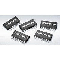
FM31L278-G Ramtron, FM31L278-G Datasheet - Page 6

FM31L278-G
Manufacturer Part Number
FM31L278-G
Description
FRAM, MPU SUPPORT, 256K, RTC, SOIC14
Manufacturer
Ramtron
Datasheet
1.FM31L272-G.pdf
(26 pages)
Specifications of FM31L278-G
Memory Size
256Kbit
Nvram Features
RTC
Supply Voltage Range
2.7V To 3.6V
Memory Case Style
SOIC
No. Of Pins
14
Operating Temperature Range
-40°C To +85°C
Package / Case
SOIC
Mounting Style
SMD/SMT
Memory Configuration
32768 X 8
Interface Type
I2C, Serial, 2-Wire
Rohs Compliant
Yes
Number Of Voltages Monitored
1
Monitored Voltage
2.6 V or 2.9 V
Output Type
Active Low, Open Drain
Manual Reset
Resettable
Watchdog
Watchdog
Battery Backup Switching
Yes
Power-up Reset Delay (typ)
200 ms
Supply Voltage (max)
3.6 V
Supply Voltage (min)
2.7 V
Supply Current (typ)
1500 uA
Power Fail Detection
Yes
Lead Free Status / RoHS Status
Lead free / RoHS Compliant
Lead Free Status / RoHS Status
Lead free / RoHS Compliant
Available stocks
Company
Part Number
Manufacturer
Quantity
Price
Part Number:
FM31L278-G
Manufacturer:
CYPRESS/赛普拉斯
Quantity:
20 000
Company:
Part Number:
FM31L278-GTR
Manufacturer:
SIEMENS
Quantity:
124
Part Number:
FM31L278-GTR
Manufacturer:
CYPRESS
Quantity:
20 000
The voltage on the PFI input pin is compared to an
onboard 1.2V reference. When the PFI input voltage
drops below this threshold, the comparator will drive
the CAL/PFO pin to a low state. The comparator has
100 mV (max) of hysteresis to reduce noise
sensitivity, only for a rising PFI signal. For a falling
PFI edge, there is no hysteresis.
The comparator is a general purpose device and its
application is not limited to the NMI function.
The comparator is not integrated into the special
function registers except as it shares its output pin
with the CAL output. When the RTC calibration
mode is invoked by setting the CAL bit (register 00h,
bit 2), the CAL/PFO output pin will be driven with a
512 Hz square wave and the comparator will be
ignored. Since most users only invoke the calibration
mode during production, this should have no impact
on system operations using the comparator.
Note: The maximum voltage on the comparator input PFI
is limited to 3.75V under normal operating conditions.
Event Counter
The FM31L27x offers the user two battery-backed
event counters. Input pins CNT1 and CNT2 are
programmable edge detectors. Each clocks a 16-bit
counter. When an edge occurs, the counters will
increment their respective registers. Counter 1 is
located in registers 0Dh and 0Eh, Counter 2 is
located in registers 0Fh and 10h. These register
values can be read anytime VDD is above VTP, and
they will be incremented as long as a valid VBAK
power source is provided. To read, set the RC bit
register 0Ch bit 3 to 1. This takes a snapshot of all
four counter bytes allowing a stable value even if a
count occurs during the read. The registers can be
written by software allowing the counters to be
cleared or initialized by the system. Counts are
blocked during a write operation. The two counters
can be cascaded to create a single 32-bit counter by
setting the CC control bit (register 0Ch). When
cascaded, the CNT1 input will cause the counter to
increment. CNT2 is not used in this mode.
Rev. 2.0
Jan. 2011
CNT1
CNT2
C1P
C2P
Figure 6. Event Counter
CC
16-bit Counter
16-bit Counter
The control bits for event counting are located in
register 0Ch. Counter 1 Polarity is bit C1P, bit 0;
Counter 2 Polarity is C2P, bit 1; the Cascade Control
is CC, bit 2; and the Read Counter bit is RC bit 3.
The polarity bits must be set prior to setting the
counter value(s). If a polarity bit is changed, the
counter may inadvertently increment. If the counter
pins are not being used, tie them to ground.
Serial Number
A memory location to write a 64-bit serial number is
provided. It is a writeable nonvolatile memory block
that can be locked by the user once the serial number
is set. The 8 bytes of data and the lock bit are all
accessed via the device ID for the processor
companion. Therefore the serial number area is
separate and distinct from the memory array. The
serial number registers can be written an unlimited
number of times, so these locations are general
purpose memory. However once the lock bit is set the
values cannot be altered and the lock cannot be
removed. Once locked the serial number registers can
still be read by the system.
The serial number is located in registers 11h to 18h.
The lock bit is SNL, register 0Bh bit 7. Setting the
SNL bit to a 1 disables writes to the serial number
registers, and the SNL bit cannot be cleared.
Real-Time Clock Operation
The real-time clock (RTC) is a timekeeping device
that can be battery or capacitor backed for
permanently-powered operation. It offers a software
calibration feature that allows high accuracy.
The RTC consists of an oscillator, clock divider, and
a register system for user access. It divides down the
32.768 kHz time-base and provides a minimum
resolution of seconds (1Hz). Static registers provide
the user with read/write access to the time values. It
includes registers for seconds, minutes, hours, day-
of-the-week, date, months, and years. A block
diagram (Figure 7) illustrates the RTC function.
The user registers are synchronized with the
timekeeper core using R and W bits in register 00h
described below. Changing the R bit from 0 to 1
transfers timekeeping information from the core into
holding registers that can be read by the user. If a
timekeeper update is pending when R is set, then the
core will be updated prior to loading the user
registers. The registers are frozen and will not be
updated again until the R bit is cleared to 0. R is used
for reading the time.
Setting the W bit to 1 locks the user registers.
Clearing it to 0 causes the values in the user registers
FM31L278/L276/L274/L272 - 3V I2C Companion
Page 6 of 26


