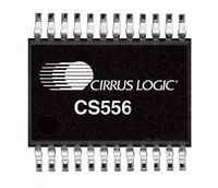
CS5560-ISZR Cirrus Logic Inc, CS5560-ISZR Datasheet - Page 3

CS5560-ISZR
Manufacturer Part Number
CS5560-ISZR
Description
IC 50 DSDS 24-bit Mux DS ADC
Manufacturer
Cirrus Logic Inc
Specifications of CS5560-ISZR
Number Of Bits
24
Data Interface
Serial
Number Of Converters
1
Power Dissipation (max)
85mW
Voltage Supply Source
Dual ±
Operating Temperature
-40°C ~ 85°C
Mounting Type
Surface Mount
Package / Case
24-SSOP
Lead Free Status / RoHS Status
Lead free / RoHS Compliant
For Use With
598-1277 - KIT BOARD FOR CDB5560 ADC598-1273 - DEV BOARD FOR CS5560 W/MUX
Lead Free Status / RoHS Status
Lead free / RoHS Compliant, Lead free / RoHS Compliant
AN314REV1
As illustrated, not every input may require an amplifier or buffer. This is because there is an on-chip buffer in the
CS556x/7x/8x. This rough charge buffer minimizes the sampling current on the input by charging the internal sam-
ple capacitor to a value very close to the input voltage using current from the supply pins rather than the input pin.
This results in much higher effective impedance on the analog input. Where the full-scale range needs to be
changed, an amplifier with gain or attenuation can be used.
4. SELECTING A MULTIPLEXER
There are several key parameters that need to be considered when selecting a MUX device. These include the “on”
resistance, on/off capacitance, and switching speed. The on resistance should be as low as possible in order to
assure that the input of the ADC fully settles on every sample. The inputs of modern converters consist of an analog
switch and a sample capacitor. For most SAR converters this sample capacitor (or array of capacitors) is in the
70 pF to 100 pF range and must be charged once per conversion. For the CS556x/7x/8x, the input sample capacitor
is only 4 pF but it is sampled once every 125 nanoseconds (8 MHz sample frequency). The CS556x/7x/8x also in-
cludes a rough-charge buffer which charges the sample capacitor to near its final value before switching the sample
capacitor directly to the input pin for the fine-sample period. This greatly increases the effective input impedance of
the device. However, this fine-sample period is only 20 nanoseconds out of each 125-nanosecond sample period,
so excessive resistance in the input path may result in inadequate settling. Another reason the on resistance should
be kept low is that the on resistance of a multiplexer is nonlinear across the full-scale range of the ADC and this may
result in distortion. The lower the on resistance, the less distortion will result from this nonlinearity. As a general
rule, an on resistance of less than 10 ohms should be used in order to minimize settling delays in charging the sam-
ple capacitance of the ADC.
The second parameter that should be considered is the channel capacitance or the on and off capacitance of the
multiplexer. Typically the inputs or source of a multiplexer have a capacitance of 5 pF to 20 pF when the switch is
open. However, when an input switch closes, additional capacitance is added from the other analog-switch chan-
nels that are part of the multiplexers output/drain. This capacitance typically increases as the number of multiplexer
inputs increase. For example, a 16-to-1 MUX will usually have a higher drain capacitance than an 8-to-1 MUX.
What needs to be considered here is that the output-channel capacitance will always be charged to the previously
AIN1
AIN2
AIN3
AIN4
Figure 4. Amplifier(s) and Filter(s) Placed Before Multiplexer
MUX
ADC
AN314
3


