LP339M National Semiconductor, LP339M Datasheet - Page 2
LP339M
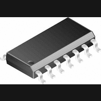
Manufacturer Part Number
LP339M
Description
Voltage Comparator IC
Manufacturer
National Semiconductor
Specifications of LP339M
No. Of Comparators
4
Response Time
8µs
No. Of Pins
14
Output Type
CMOS
Mounting Type
Surface Mount
Peak Reflow Compatible (260 C)
No
No. Of Circuits
4
Leaded Process Compatible
No
Lead Free Status / RoHS Status
Contains lead / RoHS non-compliant
Available stocks
Company
Part Number
Manufacturer
Quantity
Price

Part Number:
LP339M
Manufacturer:
NS/国半
Quantity:
20 000
Part Number:
LP339M/NOPB
Manufacturer:
NS/国半
Quantity:
20 000
Part Number:
LP339MX
Manufacturer:
NS/国半
Quantity:
20 000
Company:
Part Number:
LP339MX/NOPB
Manufacturer:
NS
Quantity:
598
Part Number:
LP339MX/NOPB
Manufacturer:
TI/德州仪器
Quantity:
20 000


www.national.com
Input Offset Voltage
Input Bias Current
Input Offset Current
Input Common
Mode Voltage Range
Supply Current
Voltage Gain
Large Signal
Response Time
Response Time
Output Sink Current
Output Leakage Current
Input Offset Voltage
Input Offset Current
Input Bias Current
Input Common
Mode Voltage Range
Output Sink Current
Output Leakage Current
Differential Input Voltage
(V+ = 5 V
Electrical Characteristics
Note 1: Absolute Maximum Ratings indicate limits beyond which damage to the device may occur. Operating Ratings indicate conditions for which the device is func-
tional, but do not guarantee specific performance limits.
Note 2: For elevated temperature operation, T
either device is soldered in a printed circuit board in a still air environment. The low bias dissipation and the “ON-OFF” characteristic of the outputs keeps the chip
dissipation very small (P
Note 3: Short circuits from the output to V
Note 4: This input current will only exist when the voltage at any of the input leads is driven negative. It is due to the collector-base junction of the input PNP tran-
sistors becoming forward biased and thereby acting as input clamp diodes. In addition to this diode action, there is also lateral NPN parasitic transistor action on the
IC chip. This transistor action can cause the output voltage of the comparators to go to the V+ voltage level (or to ground for a large input overdrive) for the time du-
ration that an input is driven negative. This is not destructive and normal output states will re-establish when the input voltage, which is negative, again returns to a
value greater than −0.3 V
Note 5: These specifications apply for V
tested. These parameters are not used to calculate outgoing AQL.
Note 6: The direction of the input current is out of the IC due to the PNP input stage. This current is essentially constant, independent of the state of the output, so
no loading change exists on the reference or the input lines as long as the common-mode range is not exceeded.
Note 7: The input common-mode voltage or either input voltage should not be allowed to go negative by more than 0.3V. The upper end of the common-mode volt-
age range is V
Note 8: The response time specified is for a 100 mV input step with 5 mV overdrive. For larger overdrive signals 1.3 µs can be obtained. See Typical Performance
Characteristics section.
Absolute Maximum Ratings
If Military/Aerospace specified devices are required,
please contact the National Semiconductor Sales Office/
Distributors for availability and specifications.
Supply Voltage
Differential Input Voltage
Input Voltage
Power Dissipation (Note 2)
Output Short Circuit to GND (Note 3)
Input Current V
Molded DIP
DC
Parameter
) (Note 5)
+
−1.5V (T
IN
<
−0.3 V
D
A
DC
= 25˚C), but either or both inputs can go to 30 V
100 mW), provided the output transistors are allowed to saturate.
(T
A
= 25˚C).
DC
(Note 4)
T
I
Output in the Linear Range, T
I
T
R
V
R
V
V
V
V
T
V
V
(Note 10)
I
I
Single Supply
V
V
All V
+
IN
IN
IN
IN
= 5V
A
A
A
L
O
L
IN
RL
RL
IN
O
IN
IN
IN
+
(+) or I
(+)−I
(+)−I
(+) or I
= 25˚C (Note 10)
= 25˚C (Note 7)
= 25˚C (Note 12)
= Infinite on all Comparators, T
= 15 k , V
= 0.4 V
can cause excessive heating and eventual destruction. The maximum output current is approximately 50 mA.
= TTL Logic Swing, V
(−) = 1 V
(+) = 1 V
(−) = 1 V
(+) = 1 V
= 1 V
= 5 V
= 5 V
DC
j
IN’s
max is 125˚C for the LP339.
and 0˚C T
IN
IN
DC
DC
(−), T
(−)
−0.3 V
0 V
36 V
IN
DC
IN
DC
(−) with the
DC
DC
(−) with Output in Linear Range
DC
DC
, R
, R
DC
to 11 V
+
, V
, V
, V
, V
DC
= 15 V
L
L
A
A
= 5.1 k , T
= 5.1 k , T
(Note 1)
= 25˚C
DC
(or V
IN
IN
IN
IN
or
70˚ C, unless otherwise stated. The temperature extremes are guaranteed but not 100% production
Continuous
(+) = 0, V
(−) = 0, V
(+) = 0, V
(−) = 0, V
to 36 V
DC
±
±
DC
570 mW
−
18 V
36 V
50 mA
Conditions
,
on split supplies) (Note 9)
, T
REF
A
A
A
DC
DC
DC
DC
O
O
O
O
= 25˚C
= 25˚C
= 25˚C (Note 8)
= 2 V
= 5 V
= 2 V
= 30 V
= 1.4 V
ja
without damage.
A
(junction to ambient) is 175˚C/W for the LP339N and 120˚C/W for the LP339M when
2
= 25˚C (Note 6)
DC
DC
DC
A
DC
= 25˚C
DC
Operating Temperature Range
Storage Temperature Range
Soldering Information:
See AN-450 “Surface Mounting Methods and Their Effect on
Product Reliability” for other methods of soldering surface
mount devices.
,
, T
,
Dual-In-Line Package (10 sec.)
S.O. Package:
A
= 25˚C
Vapor Phase (60 sec.)
Infrared (15 sec.)
0.20
Min
15
10
0
0
±
0.70
Typ
500
2.5
1.3
0.1
±
60
30
±
0.5
8
4
2
1
V+−1.5
V+−2.0
Max
±
−65˚ to +150˚C
100
1.0
±
±
±
25
40
36
15
5
5
9
0˚C to +70˚C
+260˚C
+215˚C
+220˚C
mV
mA
mA
mV
mA
Units
V/mV
nA
nA
µA
µSec
µSec
nA
nA
nA
µA
V
V
V
DC
DC
DC
DC
DC
DC
DC
DC
DC
DC
DC
DC
DC
DC
DC
Related parts for LP339M
Image
Part Number
Description
Manufacturer
Datasheet
Request
R

Part Number:
Description:
LP LOW OFFSET VOLT DUAL COMP
Manufacturer:
National Semiconductor
Part Number:
Description:
National Semiconductor [8-Bit D/A Converter]
Manufacturer:
National Semiconductor
Datasheet:
Part Number:
Description:
National Semiconductor [Media Coprocessor]
Manufacturer:
National Semiconductor
Datasheet:
Part Number:
Description:
Digitally Controlled Tone and Volume Circuit with Stereo Audio Power Amplifier, Microphone Preamp Stage and National 3D Sound
Manufacturer:
National Semiconductor
Datasheet:
Part Number:
Description:
Digitally Controlled Tone and Volume Circuit with Stereo Audio Power Amplifier, Microphone Preamp Stage and National 3D Sound
Manufacturer:
National Semiconductor
Datasheet:
Part Number:
Description:
AC97 Rev 2 Codec with Sample Rate Conversion and National 3D Sound
Manufacturer:
National Semiconductor
Part Number:
Description:
Manufacturer:
National Semiconductor
Datasheet:
Part Number:
Description:
Manufacturer:
National Semiconductor
Datasheet:
Part Number:
Description:
General Purpose, Low Voltage, Low Power, Rail-to-Rail Output Operational Amplifiers
Manufacturer:
National Semiconductor
Datasheet:
Part Number:
Description:
8-bit 20 MSPS flash A/D converter.
Manufacturer:
National Semiconductor
Datasheet:
Part Number:
Description:
Low Noise Quad Operational Amplifier
Manufacturer:
National Semiconductor
Datasheet:
Part Number:
Description:
Quad Differential Line Receivers
Manufacturer:
National Semiconductor
Datasheet:
Part Number:
Description:
Quad High Speed Trapezoidal? Bus Transceiver
Manufacturer:
National Semiconductor
Datasheet:
Part Number:
Description:
Dual Line Receiver
Manufacturer:
National Semiconductor
Datasheet: