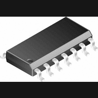
LP339M National Semiconductor, LP339M Datasheet - Page 4

LP339M
Manufacturer Part Number
LP339M
Description
Voltage Comparator IC
Manufacturer
National Semiconductor
Specifications of LP339M
No. Of Comparators
4
Response Time
8µs
No. Of Pins
14
Output Type
CMOS
Mounting Type
Surface Mount
Peak Reflow Compatible (260 C)
No
No. Of Circuits
4
Leaded Process Compatible
No
Lead Free Status / RoHS Status
Contains lead / RoHS non-compliant
Available stocks
Company
Part Number
Manufacturer
Quantity
Price
Part Number:
LP339M
Manufacturer:
NS/国半
Quantity:
20 000
Part Number:
LP339M/NOPB
Manufacturer:
NS/国半
Quantity:
20 000
Part Number:
LP339MX
Manufacturer:
NS/国半
Quantity:
20 000
Company:
Part Number:
LP339MX/NOPB
Manufacturer:
NS
Quantity:
598
Part Number:
LP339MX/NOPB
Manufacturer:
TI/德州仪器
Quantity:
20 000
www.national.com
Application Hints
All pins of any unused comparators should be tied to the
negative supply.
The bias network of the LP339 establishes a drain current
which is independent of the magnitude of the power supply
voltage over the range of from 2 V
It is usually unnecessary to use a bypass capacitor across
the power supply line.
The differential input voltage may be larger than V+ without
damaging the device. Protection should be provided to pre-
vent the input voltages from going negative more than −0.3
V
in the application section.
The output section of the LP339 has two distinct modes of
operation-a Darlington mode and a grounded emitter mode.
This unique drive circuit permits the LP339 to sink 30 mA at
V
(grounded emitter mode). Figure 1 is a simplified schematic
diagram of the LP339 output section.
Typical Applications
DC
O
= 2 V
(at 25˚C). An input clamp diode can be used as shown
DC
(Darlington mode) and 700 µA at V
DC
(V
+
to 30 V
= 15 V
DC
DC
)
.
O
= 0.4 V
One-Shot Multivibrator
DC
4
Notice that the output section is configured in a Darlington
connection (ignoring Q3). Therefore, if the output voltage is
held high enough (V
output current is limited only by the product of the betas of
Q1, Q2 and I1 (and the 60
capable of driving LED’s, relays, etc. in this mode while
maintaining an ultra-low power supply current of typically
60 µA.
If transistor Q3 were omitted, and the output voltage allowed
to drop below about 0.8 V
and the output current would drop to zero. The circuit would,
therefore, be unable to “pull” low current loads down to
ground (or the negative supply, if used). Transistor Q3 has
been included to bypass transistor Q1 under these condi-
tions and apply the current I1 directly to the base of Q2. The
output sink current is now approximately I1 times the beta of
Q2 (700 µA at V
its a bi-modal characteristic with a smooth transition be-
tween modes. (See Output Sink Current graphs in Typical
Performance Characteristics section.)
It is also important to note that in both cases the output is an
uncommitted collector. Therefore, many collectors can be
tied together to provide an output OR’ing function. An output
pull-up resistor can be connected to any available power
supply voltage within the permitted power supply voltage
range and there is no restriction on this voltage due to the
magnitude of the voltage which is applied to the V+ terminal
of the LP339 package.
O
= 0.4 V
O
1 V
DS005226-13
DC
FIGURE 1.
DC
). The output of the LP339 exhib-
DC
R
), Q1 is not saturated and the
, transistor Q1 would saturate
SAT
of Q2). The LP339 is thus
DS005226-11


