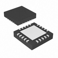
PIC16HV785-E/ML Microchip Technology, PIC16HV785-E/ML Datasheet - Page 3

PIC16HV785-E/ML
Manufacturer Part Number
PIC16HV785-E/ML
Description
3.5KB Flash, 128 RAM, 18 I/O 20 QFN 4x4mm TUBE
Manufacturer
Microchip Technology
Series
PIC® 16Fr
Datasheets
1.PIC16F616T-ISL.pdf
(8 pages)
2.PIC16F785-ISS.pdf
(206 pages)
3.PIC16F785-ISS.pdf
(10 pages)
4.PIC16F785-ISS.pdf
(28 pages)
Specifications of PIC16HV785-E/ML
Core Processor
PIC
Core Size
8-Bit
Speed
20MHz
Peripherals
Brown-out Detect/Reset, POR, PWM, WDT
Number Of I /o
17
Program Memory Size
3.5KB (2K x 14)
Program Memory Type
FLASH
Eeprom Size
256 x 8
Ram Size
128 x 8
Voltage - Supply (vcc/vdd)
2 V ~ 5.5 V
Data Converters
A/D 14x10b
Oscillator Type
Internal
Operating Temperature
-40°C ~ 125°C
Package / Case
20-VQFN Exposed Pad, 20-HVQFN, 20-SQFN, 20-DHVQFN
Processor Series
PIC16H
Core
PIC
Data Bus Width
8 bit
Data Ram Size
128 B
Interface Type
RS- 232, USB
Maximum Clock Frequency
32 MHz
Number Of Programmable I/os
18
Number Of Timers
3
Maximum Operating Temperature
+ 125 C
Mounting Style
SMD/SMT
3rd Party Development Tools
52715-96, 52716-328, 52717-734
Development Tools By Supplier
PG164130, DV164035, DV244005, DV164005, PG164120, ICE2000, DV164120, DM163029
Minimum Operating Temperature
- 40 C
On-chip Adc
10 bit, 14 Channel
Lead Free Status / RoHS Status
Lead free / RoHS Compliant
For Use With
AC164324 - MODULE SKT FOR MPLAB 8DFN/16QFN
Connectivity
-
Lead Free Status / Rohs Status
Details
Available stocks
Company
Part Number
Manufacturer
Quantity
Price
Company:
Part Number:
PIC16HV785-E/ML
Manufacturer:
LEGERITY
Quantity:
100
Silicon Errata Issues
1. Module: Two-Phase PWM
© 2009 Microchip Technology Inc.
Note:
The Complementary mode is not supported due to
the nature and extent of the Complementary mode
anomalies. Complementary mode should be used
for evaluation purposes only.
1. Duty cycle by comparator feedback (COMOD
2. When the duty cycle is determined by the
3. Maximum phase switching dead time is limited
4. The shutdown condition will correctly force
5. If the dead time is not zero and PWMPH1<4:0>
Work around
None.
Affected Silicon Revisions
A2
X
= X1) is not supported.
difference between the PH1 and PH2 phase
delays (CMOD = 10), both outputs can some-
times hang low if the duty cycle is less than
20 ns or greater than the phase switching dead
time. The hang condition can only be cleared
by setting the dead time to zero.
by the PWM clock frequency (pwm_clock). At
a pwm_clock frequency of 20 MHz, the maxi-
mum dead time is about 35 ns. At a
pwm_clock frequency of 10 MHz, the maxi-
mum dead time is about 80 ns. The relation-
ship between maximum dead time and
pwm_clock frequency is approximately linear.
PH1 false (low output at PH1 flop before the
inverting XOR gate). PH2 will be incorrectly
forced true (high output at PH2 flop before
inverting XOR gate).
= PWMPH2<4:0> then both phase outputs will
be driven false (PH1 and PH2 low before invert-
ing XOR gate). If the dead time is zero and
PWMPH1<4:0> = PWMPH2<4:0>, then phase
1 will be driven true (PH2 high) for all but one
pwm_clock cycles every PWM period.
This document summarizes all silicon
errata issues from all revisions of silicon,
previous as well as current. Only the
issues indicated by the shaded column in
the following tables apply to the current
silicon revision (A4).
A3
X
(Complementary Mode)
2. Module: Two-Phase PWM (Two-Phase
3. Module: Capture/Compare/PWM (CCP)
1. If the PWMASE bit is set when the PASEN bit
2. In normal two-phase operation when the
Work around
None.
Affected Silicon Revisions
The first capture will occur one edge too early if the
RC5/CCP1 input is high when selecting the CCP
mode
(CCP1CON<3:0> = 0110) or every 16th edge
(CCP1CON<3:0> = 0111). Subsequent captures
will occur properly.
Work around
None.
Affected Silicon Revisions
A2
A2
X
X
PIC16F785/HV785
is cleared, then the PWMASE bit will be stuck
high and the PWM will be frozen in shutdown.
Shutdown can only be cleared by first setting
the PASEN bit high then clearing the shutdown
condition (RA2/INT input must be high) so the
PWMASE bit can be cleared.
output is inverted, the leading edge is delayed
by about 10 ns and the trailing edge occurs
about 7 ns early. When the phase delay is set
to maximum, the leading edge is delayed
about 8 ns. The net result of these two
phenomena is that at 20 MHz F
inverted output at maximum phase delay will
not be generated.
A3
A3
to
X
X
Mode)
capture
either
every
DS80234E-page 3
OSC
, a blanked
4th
edge


