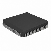
PIC16LC926-I/L Microchip Technology, PIC16LC926-I/L Datasheet - Page 77

PIC16LC926-I/L
Manufacturer Part Number
PIC16LC926-I/L
Description
IC,MICROCONTROLLER,8-BIT,PIC CPU,CMOS,LDCC,68PIN,PLASTIC
Manufacturer
Microchip Technology
Series
PIC® 16Cr
Specifications of PIC16LC926-I/L
Rohs Compliant
YES
Core Processor
PIC
Core Size
8-Bit
Speed
20MHz
Connectivity
I²C, SPI
Peripherals
Brown-out Detect/Reset, LCD, POR, PWM, WDT
Number Of I /o
25
Program Memory Size
14KB (8K x 14)
Program Memory Type
OTP
Ram Size
336 x 8
Voltage - Supply (vcc/vdd)
2.5 V ~ 5.5 V
Data Converters
A/D 5x10b
Oscillator Type
External
Operating Temperature
-40°C ~ 85°C
Package / Case
68-PLCC
Processor Series
PIC16LC
Core
PIC
Data Bus Width
8 bit
Data Ram Size
336 B
Interface Type
I2C, SPI
Maximum Clock Frequency
20 MHz
Number Of Programmable I/os
25
Number Of Timers
1 x 16 bit
Operating Supply Voltage
2.5 V to 5.5 V
Maximum Operating Temperature
+ 85 C
Mounting Style
SMD/SMT
3rd Party Development Tools
52715-96, 52716-328, 52717-734
Development Tools By Supplier
ICE2000
Minimum Operating Temperature
- 40 C
On-chip Adc
5 bit
Lead Free Status / RoHS Status
Lead free / RoHS Compliant
Eeprom Size
-
Lead Free Status / Rohs Status
Details
Available stocks
Company
Part Number
Manufacturer
Quantity
Price
Company:
Part Number:
PIC16LC926-I/L
Manufacturer:
TI
Quantity:
1 200
Company:
Part Number:
PIC16LC926-I/L
Manufacturer:
Microchip Technology
Quantity:
10 000
10.0
The Analog-to-Digital (A/D) Converter module has five
inputs.
The analog input charges a sample and hold capacitor.
The output of the sample and hold capacitor is the input
into the converter. The converter then generates a dig-
ital result of this analog level via successive approxima-
tion. The A/D conversion of the analog input signal
results in a corresponding 10-bit digital number. The
A/D module has high and low voltage reference input,
that is software selectable to some combination of V
V
The A/D converter has a unique feature of being able
to operate while the device is in SLEEP mode. To
operate in SLEEP, the A/D clock must be derived from
the A/D’s internal RC oscillator.
REGISTER 10-1:
SS
2001 Microchip Technology Inc.
, RA2 or RA3.
ANALOG-TO-DIGITAL
CONVERTER (A/D) MODULE
bit 7-6
bit 5-3
bit 2
bit 1
bit 0
ADCON0 REGISTER (ADDRESS: 1Fh)
ADCS<1:0>: A/D Conversion Clock Select bits
00 = F
01 = F
10 = F
11 = F
CHS<2:0>: Analog Channel Select bits
000 = channel 0 (RA0/AN0)
001 = channel 1 (RA1/AN1)
010 = channel 2 (RA2/AN2)
011 = channel 3 (RA3/AN3)
100 = channel 4 (RA5/AN4)
GO/DONE: A/D Conversion Status bit
If ADON = 1:
1 = A/D conversion in progress (setting this bit starts the A/D conversion)
0 = A/D conversion not in progress (this bit is automatically cleared by hardware when the A/D
Unimplemented: Read as '0'
ADON: A/D On bit
1 = A/D converter module is operating
0 = A/D converter module is shut-off and consumes no operating current
bit 7
Legend:
R = Readable bit
- n = Value at POR
ADCS1
R/W-0
conversion is complete)
OSC
OSC
OSC
RC
(clock derived from the internal A/D module RC oscillator)
/2
/8
/32
ADCS0
R/W-0
R/W-0
CHS2
Preliminary
DD
W = Writable bit
’1’ = Bit is set
,
R/W-0
CHS1
The A/D module has four registers. These registers
are:
• A/D Result High Register (ADRESH)
• A/D Result Low Register (ADRESL)
• A/D Control Register0 (ADCON0)
• A/D Control Register1 (ADCON1)
The ADCON0 register, shown in Register 10-1, con-
trols the operation of the A/D module. The ADCON1
register, shown in Register 10-2, configures the func-
tions of the port pins. The port pins can be configured
as analog inputs (RA3 can also be the voltage refer-
ence), or as digital I/O.
Additional information on using the A/D module can be
found in the PICmicro™ Mid-Range MCU Family
Reference Manual (DS33023).
R/W-0
CHS0
U = Unimplemented bit, read as ‘0’
’0’ = Bit is cleared
PIC16C925/926
GO/DONE
R/W-0
x = Bit is unknown
U-0
—
DS39544A-page 75
R/W-0
ADON
bit 0


