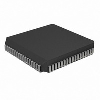
PIC16LC926-I/L Microchip Technology, PIC16LC926-I/L Datasheet - Page 96

PIC16LC926-I/L
Manufacturer Part Number
PIC16LC926-I/L
Description
IC,MICROCONTROLLER,8-BIT,PIC CPU,CMOS,LDCC,68PIN,PLASTIC
Manufacturer
Microchip Technology
Series
PIC® 16Cr
Specifications of PIC16LC926-I/L
Rohs Compliant
YES
Core Processor
PIC
Core Size
8-Bit
Speed
20MHz
Connectivity
I²C, SPI
Peripherals
Brown-out Detect/Reset, LCD, POR, PWM, WDT
Number Of I /o
25
Program Memory Size
14KB (8K x 14)
Program Memory Type
OTP
Ram Size
336 x 8
Voltage - Supply (vcc/vdd)
2.5 V ~ 5.5 V
Data Converters
A/D 5x10b
Oscillator Type
External
Operating Temperature
-40°C ~ 85°C
Package / Case
68-PLCC
Processor Series
PIC16LC
Core
PIC
Data Bus Width
8 bit
Data Ram Size
336 B
Interface Type
I2C, SPI
Maximum Clock Frequency
20 MHz
Number Of Programmable I/os
25
Number Of Timers
1 x 16 bit
Operating Supply Voltage
2.5 V to 5.5 V
Maximum Operating Temperature
+ 85 C
Mounting Style
SMD/SMT
3rd Party Development Tools
52715-96, 52716-328, 52717-734
Development Tools By Supplier
ICE2000
Minimum Operating Temperature
- 40 C
On-chip Adc
5 bit
Lead Free Status / RoHS Status
Lead free / RoHS Compliant
Eeprom Size
-
Lead Free Status / Rohs Status
Details
Available stocks
Company
Part Number
Manufacturer
Quantity
Price
Company:
Part Number:
PIC16LC926-I/L
Manufacturer:
TI
Quantity:
1 200
Company:
Part Number:
PIC16LC926-I/L
Manufacturer:
Microchip Technology
Quantity:
10 000
PIC16C925/926
11.4.1
The LCDSE register is used to select the pin function
for groups of pins. The selection allows each group of
pins to operate as either LCD drivers or digital only
pins. To configure the pins as a digital port, the corre-
sponding bits in the LCDSE register must be cleared.
trols the data direction. Any bit set in the LCDSE regis-
ter overrides any bit settings in the corresponding TRIS
register.
REGISTER 11-4:
DS39544A-page 94
If the pin is a digital I/O the corresponding TRIS bit con-
Note 1: On a Power-on Reset, these pins are
2: The LMUX1:LMUX0 takes precedence
bit 7
bit 6
bit 5
bit 4
bit 3
bit 2
bit 1
bit 0
SEGMENT ENABLES
configured as LCD drivers.
over the LCDSE bit settings for pins RD7,
RD6 and RD5.
LCDSE REGISTER (ADDRESS 10Dh)
bit 7
SE29: Pin Function Select
1 = Pins have LCD drive function
0 = Pins have digital Input function
SE27: Pin Function Select
1 = Pins have LCD drive function
0 = Pins have LCD drive function
1 = Pins have LCD drive function
0 = Pins have digital Input function
SE16: Pin Function Select
1 = Pins have LCD drive function
0 = Pins have digital Input function
SE12: Pin Function Select
1 = Pins have LCD drive function
0 = Pins have digital Input function
SE9: Pin Function Select
1 = Pins have LCD drive function
0 = Pins have digital Input function
SE5: Pin Function Select
1 = Pins have LCD drive function
0 = Pins have digital Input function
SE0: Pin Function Select
1 = Pins have LCD drive function
0 = Pins have digital Input function
Legend:
R = Readable bit
- n = Value at POR
SE20: Pin Function Select
R/W-1
SE29
R/W-1
SE27
R/W-1
SE20
Preliminary
W = Writable bit
’1’ = Bit is set
RG7/SEG28 and RE7/SEG27
RF7/SEG19 - RF4/SEG16
RF3/SEG15 - RF0/SEG12
RE6/SEG11 - RE4/SEG09
RE3/SEG08 - RE0/SEG05
RD4/SEG04 - RD0/SEG00
RD7/COM1/SEG31 - RD5/COM3/SEG29
RG6/SEG26 - RG0/SEG20
R/W-1
SE16
EXAMPLE 11-1:
EXAMPLE 11-2:
BCF
BSF
BSF
BCF
MOVLW 0x87
MOVWF LCDSE
. . .
BCF
BSF
BCF
BCF
MOVLW 0xFF
MOVWF LCDSE
. . .
U = Unimplemented bit, read as ‘0’
’0’ = Bit is cleared
STATUS,RP0
STATUS,RP1
LCDCON,LMUX1 ;Select Static MUX
LCDCON,LMUX0 ;
STATUS,RP0
STATUS,RP1
LCDCON,LMUX1 ;Select 1/3 MUX
LCDCON,LMUX0 ;
R/W-1
SE12
STATIC MUX WITH 32
SEGMENTS
ONE-THIRD DUTY CYCLE
WITH 13 SEGMENTS
R/W-1
SE9
;Select Bank 2
;
;Make PortD,E,F,G
;LCD pins
;configure rest of LCD
;Select Bank 2
;
;Make PORTD<7:0> &
;PORTE<6:0> LCD pins
;configure rest of LCD
2001 Microchip Technology Inc.
x = Bit is unknown
R/W-1
SE5
R/W-1
SE0
bit 0


