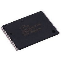
S29GL032A10TFIR40 Spansion Inc., S29GL032A10TFIR40 Datasheet - Page 64

S29GL032A10TFIR40
Manufacturer Part Number
S29GL032A10TFIR40
Description
Flash - NOR IC
Manufacturer
Spansion Inc.
Datasheet
1.S29GL032A10TFIR40.pdf
(88 pages)
Specifications of S29GL032A10TFIR40
Memory Size
32Mbit
Memory Configuration
64K X 8
Ic Interface Type
Parallel
Access Time
100ns
Memory Case Style
TSOP
No. Of Pins
48
Operating Temperature Range
-40°C To +85°C
Page/burst Read Access
25ns
- Current page: 64 of 88
- Download datasheet (2Mb)
62
DQ3: Sector Erase Timer
DQ1: Write-to-Buffer Abort
In all these cases, the system must write the reset command to return the device
to the reading the array (or to erase-suspend-read if the device was previously
in the erase-suspend-program mode).
After writing a sector erase command sequence, the system may read DQ3 to de-
termine whether or not erasure has begun. (The sector erase timer does not
apply to the chip erase command.) If additional sectors are selected for erasure,
the entire time-out also applies after each additional sector erase command.
When the time-out period is complete, DQ3 switches from a “0” to a “1.” If the
time between additional sector erase commands from the system can be as-
sumed to be less than 50 µs, the system need not monitor DQ3. See also the
Sector Erase Command Sequence section.
After the sector erase command is written, the system should read the status of
DQ7 (Data# Polling) or DQ6 (Toggle Bit I) to ensure that the device has accepted
the command sequence, and then read DQ3. If DQ3 is “1,” the Embedded Erase
algorithm has begun; all further commands (except Erase Suspend) are ignored
until the erase operation is complete. If DQ3 is “0,” the device will accept addi-
tional sector erase commands. To ensure the command has been accepted, the
system software should check the status of DQ3 prior to and following each sub-
sequent sector erase command. If DQ3 is high on the second status check, the
last command might not have been accepted.
Table 27
DQ1 indicates whether a Write-to-Buffer operation was aborted. Under these
conditions DQ1 produces a “1”. The system must issue the Write-to-Buffer-Abort-
Reset command sequence to return the device to reading array data. See Write
Buffer section for more details.
shows the status of DQ3 relative to the other status bits.
S29GLxxxA MirrorBit™ Flash Family
A d v a n c e
I n f o r m a t i o n
S29GLxxxA_00_A2 January 28, 2005
Related parts for S29GL032A10TFIR40
Image
Part Number
Description
Manufacturer
Datasheet
Request
R

Part Number:
Description:
Flash 3V 32Mb Float Gate two address 90s
Manufacturer:
Spansion Inc.
Datasheet:

Part Number:
Description:
Flash 3V 64Mb Float Gate two address 90s
Manufacturer:
Spansion Inc.
Datasheet:

Part Number:
Description:
Flash 3V 64Mb Float Gate standard config 90s
Manufacturer:
Spansion Inc.
Datasheet:

Part Number:
Description:
Flash 3V 1 Gb Mirrorbit highest address120ns
Manufacturer:
Spansion Inc.
Datasheet:

Part Number:
Description:
Flash 3V 256Mb Mirrorbit highest address110ns
Manufacturer:
Spansion Inc.
Datasheet:

Part Number:
Description:
Flash 3V 64Mb Float Gate highest address 90s
Manufacturer:
Spansion Inc.
Datasheet:

Part Number:
Description:
Flash 3V 512Mb Mirrorbit lowest address100ns
Manufacturer:
Spansion Inc.
Datasheet:

Part Number:
Description:
Flash 3V 32Mb Float Gate highest address 90s
Manufacturer:
Spansion Inc.
Datasheet:

Part Number:
Description:
Flash 3V 64Mb Float Gate highest address 90s
Manufacturer:
Spansion Inc.
Datasheet:

Part Number:
Description:
Flash 3V 1 Gb Mirrorbit highest address110ns
Manufacturer:
Spansion Inc.
Datasheet:

Part Number:
Description:
Flash 3V 256Mb Mirrorbit lowest address110ns
Manufacturer:
Spansion Inc.
Datasheet:

Part Number:
Description:
Flash 3V 512Mb Mirrorbit highest address110ns
Manufacturer:
Spansion Inc.
Datasheet:

Part Number:
Description:
Flash 3V 128Mb Mirrorbit lowest address110ns
Manufacturer:
Spansion Inc.
Datasheet:

Part Number:
Description:
Flash 3V 64Mb Float Gate standard config 70s
Manufacturer:
Spansion Inc.

Part Number:
Description:
IC, FLASH, 1MBIT, 70NS, LCC-32
Manufacturer:
Spansion Inc.
Datasheet:


