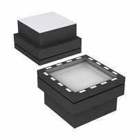
ADIS16060BCCZ Analog Devices Inc, ADIS16060BCCZ Datasheet - Page 10

ADIS16060BCCZ
Manufacturer Part Number
ADIS16060BCCZ
Description
IC GYROSCOPE YAW RATE SPI 16LGA
Manufacturer
Analog Devices Inc
Datasheet
1.ADIS16060PCBZ.pdf
(12 pages)
Specifications of ADIS16060BCCZ
Range °/s
±80°/s
Sensitivity
0.0122°/sec/LSB
Typical Bandwidth
1kHz
Voltage - Supply
4.75 V ~ 5.25 V
Current - Supply
4.3mA
Output Type
SPI
Operating Temperature
-40°C ~ 105°C
Package / Case
16-LGA
No. Of Axes
1
Sensor Case Style
LGA
No. Of Pins
16
Supply Voltage Range
4.75V To 5.25V
Operating Temperature Range
-40°C To +105°C
Msl
MSL 1 - Unlimited
Acceleration Range
2000g
Lead Free Status / RoHS Status
Lead free / RoHS Compliant
For Use With
ADIS16060/PCBZ - BOARD EVAL FOR ADIS16060
Lead Free Status / RoHS Status
Lead free / RoHS Compliant, Lead free / RoHS Compliant
ADIS16060
BASIC OPERATION
The ADIS16060 is designed for simple integration into indus-
trial system designs, requiring only a 5 V power supply, two
mode select lines, and three serial communications lines. The
SPI handles all digital I/O communication in the ADIS16060.
SERIAL PERIPHERAL INTERFACE (SPI)
The ADIS16060 SPI port includes five signals: Mode Select 1
( MSEL1 ), Mode Select 2 ( MSEL2 ), serial clock (SCLK), data
input (DIN), and data output (DOUT). The MSEL1 line is used
when reading data out of the sensor (DOUT), and the MSEL2
line is used when configuring the sensor (DIN).
Selecting Output Data
Refer to Table 5 to determine the appropriate DIN bit sequence
based on the required data source. Table 2 and Figure 3 provide
the necessary timing details for the input configuration sequence.
After the MSEL2 goes high, the last eight DIN bits are loaded
into the internal control register, which represents DB0 to DB7
in Table 5.
Table 5. DIN Configuration Bit Assignments
Action
Measure Angular Rate (Gyro)
Measure Temperature
Measure AIN2
Measure AIN1
Set Positive Self-Test and Output for Angular Rate
Set Negative Self-Test and Output for Angular Rate
Rev. 0 | Page 10 of 12
DB7
0
0
1
0
0
0
DB6
Output Data Access
Use Table 2 and Figure 2 to determine the appropriate timing
considerations for reading output data.
OUTPUT DATA FORMATTING
All of the output data is in an offset-binary format, which in
this case, means that the ideal output for a zero rate condition is
8192 codes. If the sensitivity is equal to +0.0122°/sec/LSB, a rate
of +10°/sec results in a change of 820 codes, and a digital rate
output of 9012 codes. If an offset error of −20°/sec is introduced,
the output is reduced by 1639 codes (if typical sensitivity is
assumed), resulting in a digital rate output of 6552 codes.
ADC CONVERSION
The internal successive approximation ADC begins the conversion
process on the falling edge of MSEL1 and starts to place data
MSB first on the DOUT line at the 6
shown in Figure 2. The entire conversion process takes 20 SCLK
cycles. After MSEL1 goes high, the acquisition process starts in
preparation for the next conversion cycle.
0
0
0
1
0
0
DB5
1
0
0
0
1
1
DB4
0
1
0
0
0
0
DB3
0
0
0
0
0
0
th
falling edge of SCLK, as
DB2
0
0
0
0
0
0
DB1
0
0
0
0
1
0
DB0
0
0
0
0
1
0


