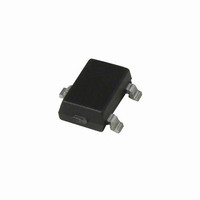
A1222EUA-T Allegro Microsystems Inc, A1222EUA-T Datasheet - Page 10

A1222EUA-T
Manufacturer Part Number
A1222EUA-T
Description
IC HALL EFFECT LATCH 3-SIP
Manufacturer
Allegro Microsystems Inc
Type
Bipolar Latchr
Datasheet
1.A1221LUA-T.pdf
(14 pages)
Specifications of A1222EUA-T
Sensing Range
150G Trip, 150G Release
Voltage - Supply
3 V ~ 24 V
Current - Supply
4mA
Current - Output (max)
25mA
Output Type
Digital, Open Drain
Features
Regulated Voltage
Operating Temperature
-40°C ~ 85°C
Package / Case
3-SIP
Hall Effect Type
Latch
Output Current
25mA
Sensor Case Style
SIP
No. Of Pins
3
Supply Voltage Range
3V To 24V
Operating Temperature Range
-40°C To +85°C
Svhc
No SVHC (15-Dec-2010)
Rohs Compliant
Yes
Lead Free Status / RoHS Status
Lead free / RoHS Compliant
A1220, A1221,
A1222, and A1223
Operation
The output of these devices switches low (turns on) when a mag-
netic field perpendicular to the Hall element exceeds the operate
point threshold, B
output voltage is V
sinking current up to the short circuit current limit, I
a minimum of 30 mA. When the magnetic field is reduced below
the release point, B
The difference in the magnetic operate and release points is the
hysteresis, B
clean switching of the output even in the presence of external
mechanical vibration and electrical noise.
Removal of the magnetic field will leave the device output
latched on if the last crossed switchpoint is B
the last crossed switch point is B
Powering-on the device in the hysteresis range (less than B
higher than B
rect state is attained after the first excursion beyond B
Figure 1. Switching behavior of latches. In panel A, on the horizontal axis, the B+ direction indicates increasing south polarity magnetic field strength,
and the B– direction indicates decreasing south polarity field strength (including the case of increasing north polarity). This behavior can be exhibited
when using a circuit such as that shown in panel B.
HYS ,
RP
V+
0
) will give an indeterminate output state. The cor-
B–
OP
of the device. This built-in hysteresis allows
OUT(SAT)
RP
(see panel A of figure 1). After turn-on, the
, the device output goes high (turns off).
. The output transistor is capable of
B
(A)
HYS
0
RP
.
Chopper Stabilized Precision Hall Effect Latches
B+
V
V
OP
CC
OUT(SAT)
, or latched off if
Functional Description
OM
OP
, which is
or B
OP
RP
and
.
Applications
It is strongly recommended that an external bypass capacitor be
connected (in close proximity to the Hall element) between the
supply and ground of the device to reduce both external noise
and noise generated by the chopper stabilization technique. As is
shown in panel B of figure 1, a 0.1 μF capacitor is typical.
Extensive applications information for Hall effect devices is
available in:
• Hall-Effect IC Applications Guide, Application Note 27701
• Guidelines for Designing Subassemblies Using Hall-Effect
Devices, Application Note 27703.1
• Soldering Methods for Allegro’s Products – SMT and Through-
Hole, Application Note 26009
All are provided in Allegro Electronic Data Book, AMS-702, and
the Allegro Web site, www.allegromicro.com.
C
0.1 μF
V
BYP
S
A122x
115 Northeast Cutoff
1.508.853.5000; www.allegromicro.com
GND
Allegro MicroSystems, Inc.
Worcester, Massachusetts 01615-0036 U.S.A.
VCC
(B)
VOUT
R
L
Output
10


