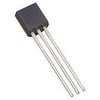
A1242EUA-I1-T Allegro Microsystems Inc, A1242EUA-I1-T Datasheet - Page 4

A1242EUA-I1-T
Manufacturer Part Number
A1242EUA-I1-T
Description
IC LATCH HALL EFFECT 3-SIP
Manufacturer
Allegro Microsystems Inc
Type
Unipolar Switchr
Datasheet
1.A1242ELHLT-I1-T.pdf
(12 pages)
Specifications of A1242EUA-I1-T
Package / Case
3-SIP
Sensing Range
80G Trip, -80G Release
Voltage - Supply
3.5 V ~ 24 V
Current - Supply
6.9mA
Output Type
Digital, Open Drain
Features
Regulated Voltage
Operating Temperature
-40°C ~ 85°C
Peak Reflow Compatible (260 C)
Yes
Termination Type
Through Hole
Supply Voltage Max
24V
No. Of Pins
3
Hall Effect Type
Latching
Supply Voltage Min
3.5V
Lead Free Status / RoHS Status
Lead free / RoHS Compliant
Current - Output (max)
-
Lead Free Status / RoHS Status
Lead free / RoHS Compliant, Lead free / RoHS Compliant
A1242
1
mum limits.
2
3
4
points. The value of dI/dt depends on the value of the bypass capacitor, if one is used, with greater capacitances resulting in lower
rates of change.
5
6
7
magnetic fields. This so-called algebraic convention supports arithmetic comparison of north and south polarity values, where the rela-
tive strength of the field is indicated by the absolute value of B, and the sign indicates the polarity of the field (for example, a –100 G
field and a 100 G field have equivalent strength, but opposite polarity).
ELECTRICAL CHARACTERISTICS
Electrical Characteristics
Supply Voltage
Supply Current
Output Slew Rate
Chopping Frequency
Power-On Time
Power-On State
Supply Zener Clamp Voltage
Supply Zener Current
Reverse Battery Current
Magnetic Characteristics
Operate Point
Release Point
Hysteresis
Typical values are at T
Maximum voltage must be adjusted for power dissipation and junction temperature; see Power Derating section.
V
The value of dI is the difference between 90% of I
For t > t
Maximum current limit is equal to the maximum I
Magnetic flux density, B, is indicated as a negative value for north-polarity magnetic fields, and as a positive value for south-polarity
CC
represents the generated voltage between the V
PO(max)
Characteristic
2 3
5
, and B
4
6
RP
A
7
= 25°C and V
< B < B
OP
, POS is undefined.
EMC (Electromagnetic Compatibility) PERFORMANCE
V
Symbol
I
Z(supply)
CC
Z(supply)
I
I
B
POS
CC(H)
dI/dt
I
V
CC(L)
B
B
t
RCC
f
PO
HYS
CC
OP
RP
C
= 12 V. Performance may vary for individual units, within the specified maximum and mini-
Two-Wire Chopper-Stabilized Hall Effect Latch
over full operating voltage and temperature ranges, unless otherwise specified
DEVICE QUALIFICATION PROGRAM
Operating, T
-I1, B < B
-I2, B < B
-I1 and -I2, B > B
R
V
t
I
V
V
South pole adjacent to branded face of device
North pole adjacent to branded face of device
B
CCL(max)
PO
CC
CC(H)
CC
S
RCC
OP
S
Contact Allegro for information.
Contact Allegro for information.
= 28 V
= 100 Ω, C
< t
= 20 mA; T
> V
– B
CC
= –18 V
PO(max)
and 10% of I
CC(MIN)
RP
pin and the GND pin.
RP
RP
+ 3 mA.
J
, dV
< 165°C
S
A
= 20 pF, no bypass capacitor
= 25°C
OP
CC
Test Conditions
/ dt > 25 mV / μs
CC(L)
, and the value of dt is time period between those two
115 Northeast Cutoff
1.508.853.5000; www.allegromicro.com
Allegro MicroSystems, Inc.
Worcester, Massachusetts 01615-0036 U.S.A.
Min.
–80
3.5
12
28
40
5
2
–
–
–
–
–
–
5
Typ.
I
CC(H)
200
–32
36
32
64
–
–
–
–
–
–
–
–
1
Max.
110
6.9
2.5
24
17
25
20
80
–5
5
–
–
–
–
mA/μs
Units
kHz
mA
mA
mA
mA
mA
μs
G
G
G
V
–
V
3


