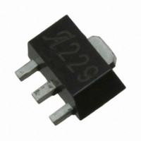
A3250LLT-T Allegro Microsystems Inc, A3250LLT-T Datasheet - Page 9

A3250LLT-T
Manufacturer Part Number
A3250LLT-T
Description
IC SW HALL EFFECT UNI SOT-89
Manufacturer
Allegro Microsystems Inc
Type
Unipolar Switchr
Specifications of A3250LLT-T
Sensing Range
50G
Voltage - Supply
4.2 V ~ 24 V
Current - Supply
10mA
Current - Output (max)
20mA
Output Type
Digital, Open Collector
Features
Regulated Voltage
Operating Temperature
-40°C ~ 150°C
Package / Case
SOT-89-3
Magnetic Type
Unipolar
Operating Supply Voltage (min)
4.2V
Operating Supply Voltage (typ)
5/9/12/15/18V
Operating Supply Voltage (max)
24V
Output Current
20mA
Mag Sensor Operate Point (g)
50Gs
Mag Sensor Hysteresis(g)
13Gs
Package Type
SOT-89
Pin Count
3 +Tab
Mounting
Surface Mount
Operating Temp Range
-40C to 150C
Operating Temperature Classification
Automotive
Lead Free Status / RoHS Status
Lead free / RoHS Compliant
A3250
A3251
Chopper-Stabilized Technique
The Hall circuit is based on a Hall element, a small sheet of
semiconductor material in which a constant bias current flows
when a constant voltage source is applied. The output takes the
form of a voltage measured across the width of the Hall element,
and has negligible value in the absence of a magnetic field.
When a magnetic field is applied with flux lines at right angles
to the current in the Hall element, a small signal voltage directly
proportional to the strength of the magnetic field occurs at the
output of the Hall element.
This small signal voltage is disproportionally small relative to
the offset produced at the input of the device. This makes it very
difficult to process the signal and maintain an accurate, reliable
output over the specified temperature and voltage range. There-
fore, it is important to reduce any distortion of the signal that
could be amplified when the signal is processed.
Chopper stabilization is a unique approach used to minimize
input offset on the Hall IC. This technique removes a key
source of output drift due to temperature and mechanical stress,
and produces a 3X reduction in offset in comparison to other,
conventional methods.
This offset reduction chopping technique is based on a sig-
nal modulation-demodulation process. The undesired offset
and
Chopper stabilization circuit (dynamic quadrature offset cancellation)
Functional Description
Field-Programmable, Chopper-Stabilized,
signal is separated from the magnetically-induced signal in the
frequency domain. The offset (and any low-frequency noise)
component of the signal can be seen as signal distortion added
after the signal modulation process has taken place. Therefore,
the DC offset is not modulated and remains a low-frequency
component. Consequently, the signal demodulation process acts
as a modulation process for the offset, causing the magnetically-
induced signal to recover its original spectrum at baseband while
the DC offset becomes a high-frequency signal. Then, the signal
passes using a low-pass filter, while the modulated DC offset is
suppressed.
The advantage of this approach is significant offset reduction,
which desensitizes the Hall IC against the effects of temperature
and mechanical stress. The disadvantage is that this technique
features a demodulator that uses a sample-and-hold block to
store and recover the signal. This sampling process can slightly
degrade the SNR (signal-to-noise ratio) by producing replicas of
the noise spectrum at the baseband. This degradation is a function
of the ratio between the white noise spectrum and the sampling
frequency. The effect of the degradation of the SNR is higher
jitter, also known as signal repeatability. However, the jitter in a
continuous-time device can be 5X that of the A3250/A3251.
Unipolar Hall-Effect Switches
Regulator
Amp
115 Northeast Cutoff, Box 15036
Allegro MicroSystems, Inc.
Worcester, Massachusetts 01615-0036 (508) 853-5000
www.allegromicro.com
8


