ISL29010IROZ-T7 Intersil, ISL29010IROZ-T7 Datasheet
ISL29010IROZ-T7
Specifications of ISL29010IROZ-T7
Available stocks


Related parts for ISL29010IROZ-T7

ISL29010IROZ-T7 Summary of contents
Page 1
... ISL29010 is specified for operation over the -40°C to +85°C ambient temperature range. Ordering Information PART NUMBER TEMP. PACKAGE (Note) RANGE (°C) ISL29010IROZ-T7* - ODFN ISL29010IROZ-EVALZ Evaluation Board *Please refer to TB347 for details on reel specifications. NOTE: These Intersil Pb-free plastic packaged products employ special Pb-free material sets; molding compounds/die attach ...
Page 2
... Thermal Information = +25°C) Thermal Resistance (Typical Note ODFN . . . . . . . . . . . . . . . . . . . . . . . . . . . . . . . . Maximum Die Temperature . . . . . . . . . . . . . . . . . . . . . . . . . . . +90°C Storage Temperature . . . . . . . . . . . . . . . . . . . . . . . .-40°C to +100°C Operating Temperature . . . . . . . . . . . . . . . . . . . . . . .-40°C to +85°C Pb-free Reflow Profile . . . . . . . . . . . . . . . . . . . . . . . . .see link below http://www.intersil.com/pbfree/Pb-FreeReflow.asp = +25° 100kΩ, unless otherwise specified, Internal Timing Mode operation (See ...
Page 3
Pin Descriptions PIN NUMBER PIN NAME 1 VDD Positive supply; connect this pin to a regulated 2.5V to 3.3V supply 2 GND Ground pin. The thermal pad is connected to the GND pin 3 REXT External resistor pin for ADC ...
Page 4
Start DEVICE ADDRESS DATA SDA SDA SDA DRIVEN BY MASTER Out CLK ...
Page 5
Register Set There are eight registers that are available in the ISL29010. Table 1 summarizes the available registers and their functions. ADDR REG NAME 7 00h COMMAND ADCE ADCPD 01h CONTROL 0 04h LSB S7 SENSOR 05h MSB S15 SENSOR ...
Page 6
Control Register 01(hex) The Read/Write control register has one function: 1. Range/Gain; Bits 3 and 2. The Full Scale Range can be adjusted by an external resistor R 2 adjusted via I C using the Gain/Range function. Gain/Range has four ...
Page 7
Number of Clock Cycles, n-bit ADC The number of clock cycles determines “n” in the n-bit ADC; 2 clock cycles is a n-bit ADC programmable in the command register in the width function. Depending on the application, a ...
Page 8
INTEGRATION TIME IN EXTERNAL TIMING MODE This timing mode is programmed in the command register 00(hex) Bit 5. External Timing Mode is recommended when integration time can be synchronized to an external signal such as a PWM to eliminate noise. ...
Page 9
... Suggested PCB Footprint It is important that the users check the “Surface Mount Assembly Guidelines for Optical Dual FlatPack No Lead (ODFN) Package” before starting ODFN product board mounting. http://www.intersil.com/data/tb/TB466.pdf Layout Considerations The ISL29010 is relatively insensitive to layout. Like other devices intended to provide excellent performance even in significantly noisy environments ...
Page 10
TO 3. SLAVE_0 1 VDD 2 GND C1 C2 4.7µF 0.1µF 3 REXT REXT ISL29010 100kΩ Typical Performance Curves 1.2 HUMAN EYE RESPONSE 1.0 0.8 0.6 ISL29010 RESPONSE 0.4 0.2 0.0 -0.2 300 400 600 WAVELENGTH ...
Page 11
Typical Performance Curves +27° lux RANGE 2.0 2.3 2.6 2.9 SUPPLY VOLTAGE (V) FIGURE 11. OUTPUT CODE FOR 0 LUX vs SUPPLY VOLTAGE 320.0 319.5 319.0 318.5 318.0 2.0 ...
Page 12
Typical Performance Curves 330 329 328 327 326 325 -60 -20 20 TEMPERATURE (°C) FIGURE 17. OSCILLATOR FREQUENCY vs TEMPERATURE 1000 VDD = 3V 900 HALOGEN 800 700 INCANDESCENT 600 500 400 300 200 100 0 0 100 200 300 ...
Page 13
... Accordingly, the reader is cautioned to verify that data sheets are current before placing orders. Information furnished by Intersil is believed to be accurate and reliable. However, no responsibility is assumed by Intersil or its subsidiaries for its use; nor for any infringements of patents or other rights of third parties which may result from its use ...
Page 14
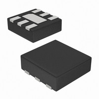
Package Outline Drawing L6.2x2.1 6 LEAD OPTICAL DUAL FLAT NO-LEAD PLASTIC PACKAGE (ODFN) Rev 0, 9/06 2.10 6 PIN 1 INDEX AREA (4X) 0.10 TOP VIEW ( 95) TYPICAL RECOMMENDED LAND PATTERN 14 ...