APDS-9008-020 Avago Technologies US Inc., APDS-9008-020 Datasheet - Page 10
APDS-9008-020
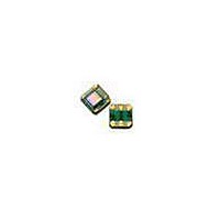
Manufacturer Part Number
APDS-9008-020
Description
IC PHOTOSENSOR AMBIENT 6CHIPLED
Manufacturer
Avago Technologies US Inc.
Type
Ambient Light Photo Sensorr
Specifications of APDS-9008-020
Package / Case
6-ChipLED - 1.60mm L x 1.50mm W x 0.55mm H
Wavelength
565nm
Output Type
Analog
Peak Wavelength
565 nm
Maximum Light Current
52 uA
Maximum Dark Current
300 nA
Maximum Rise Time
5 ms
Maximum Fall Time
5 ms
Maximum Operating Temperature
+ 85 C
Mounting Style
SMD/SMT
Product
Ambient Light Sensor
Output Current
40µA
Sensor Output
Analog
Supply Voltage Range Dc
1.6V To 5.5V
Length/height, External
0.55mm
Peak Reflow Compatible (260 C)
Yes
External Width
1.6mm
Rise Time
5ms
Rohs Compliant
Yes
External Depth
1.5mm
Leaded Process Compatible
Yes
Lead Free Status / RoHS Status
Lead free / RoHS Compliant
Lead Free Status / RoHS Status
Lead free / RoHS Compliant, Lead free / RoHS Compliant
Available stocks
Company
Part Number
Manufacturer
Quantity
Price
Company:

Part Number:
APDS-9008-020
Manufacturer:
SILICON
Quantity:
9 200
Part Number:
APDS-9008-020
Manufacturer:
AVAGO/安华高
Quantity:
20 000


Appendix A. SMT Assembly Application Note
1.0 Solder Pad, Mask and Metal Stencil Aperture
Figure A1. Stencil and PCBA
1.1 Recommended Land Pattern
Figure A2. Recommended Land Pattern
10
Mask
Aperture
Stencil
Solder
0.45
0.2
C L
0.4
0.3
0.4
Metal Stencil For
Solder Paste
Printing
Land
Pattern
PCBA
0.9
0.4
1.2 Recommended Metal Solder Stencil Aperture
It is recommended that a 0.11 mm (0.004 inches) thick
stencil be used for solder paste printing. Aperture open-
ing for shield pad is 0.4mm x 0.4mm and 0.2mm x 0.4mm
(as per land pattern). This is to ensure adequate printed
solder paste volume and no shorting.
Figure A3. Solder Stencil Aperture
1.3 Adjacent Land Keepout and Solder Mask Areas
Adjacent land keep-out is the maximum space occupied
by the unit relative to the land pattern. There should be no
other SMD components within this area.
The minimum solder resist strip width required to avoid
solder bridging adjacent pads is 0.2 mm.
Note: Wet/Liquid Photo-Imageable solder resist/mask is
recommended.
Figure A4. Adjacent Land Keepout and Solder Mask Areas
Unit: mm
Mounting
1.7
Center
Aperture
Opening
2.6
0.2 MIN.
1.6
Unit: mm
2.7
0.11
Related parts for APDS-9008-020
Image
Part Number
Description
Manufacturer
Datasheet
Request
R

Part Number:
Description:
MINIATURE SURFACE-MOUNT AMBIENT LIGHT PHOTO SENSOR
Manufacturer:
Avago Technologies US Inc.
Datasheet:

Part Number:
Description:
IC PROXIMITY SENSOR AMB LT 10QFN
Manufacturer:
Avago Technologies US Inc.
Datasheet:

Part Number:
Description:
AMBIENT LIGHT SENSOR 4CHIPLED
Manufacturer:
Avago Technologies US Inc.
Datasheet:

Part Number:
Description:
Photodiodes Sigl Conditioning IC f/ Opt Proximity Sen
Manufacturer:
Avago Technologies US Inc.
Datasheet:

Part Number:
Description:
Photodiodes Sigl Conditioning IC f/ Opt Proximity Sen
Manufacturer:
Avago Technologies US Inc.
Datasheet:

Part Number:
Description:
Photodiodes Proximity Sensor
Manufacturer:
Avago Technologies US Inc.
Datasheet:

Part Number:
Description:
INTEGRATED DIGITAL PS AND ALS
Manufacturer:
Avago Technologies US Inc.
Datasheet:

Part Number:
Description:
AMBIENT LIGHT SENSOR 6CHIPLED
Manufacturer:
Avago Technologies US Inc.
Datasheet:

Part Number:
Description:
AMBIENT LIGHT SENSOR 4CHIPLED
Manufacturer:
Avago Technologies US Inc.
Datasheet:

Part Number:
Description:
AMBIENT LIGHT SENSOR 6CHIPLED
Manufacturer:
Avago Technologies US Inc.
Datasheet:

Part Number:
Description:
OPTOCOUPLER GATE DRV 2A 16-SOIC
Manufacturer:
Avago Technologies US Inc.
Datasheet:
Part Number:
Description:
OPTOCOUPLER 2CH 2.5A 16-SOIC
Manufacturer:
Avago Technologies US Inc.
Datasheet:

Part Number:
Description:
OPTOCOUPLER GATE DRV 0.4A 16SOIC
Manufacturer:
Avago Technologies US Inc.
Datasheet:

Part Number:
Description:
OPTOCOUPLER 2.0A 250KHZ 8-DIP
Manufacturer:
Avago Technologies US Inc.
Datasheet:

Part Number:
Description:
OPTOCOUPLER 2.0A 250KHZ GW 8-SMD
Manufacturer:
Avago Technologies US Inc.
Datasheet: