AD22100KTZ Analog Devices Inc, AD22100KTZ Datasheet
AD22100KTZ
Specifications of AD22100KTZ
Available stocks


Related parts for AD22100KTZ


AD22100KTZ Summary of contents
Page 1
... The signal conditioning eliminates the need for any trimming, buffering, or linearization circuitry, greatly simplifying the system design and reducing the overall system cost. The output voltage is proportional to the temperature x the supply voltage (ratiometric). The output swings from 0. −50°C to +4. +150°C using a single +5.0 V supply. ...
Page 2
AD22100 TABLE OF CONTENTS Specifications..................................................................................... 3 Chip Specifications....................................................................... 3 Absolute Maximum Ratings............................................................ 4 ESD Caution.................................................................................. 4 Pin Configurations and Function Descriptions ........................... 5 Typical Performance Characteristics ............................................. 6 Theory of Operation ........................................................................ 7 Absolute Accuracy and Nonlinearity Specifications ............... 7 ...
Page 3
... FS (full scale) is defined as the operating temperature range −50°C to +150°C. The listed maximum specification limit applies to the guaranteed temperature range. For example, the AD22100K has a nonlinearity of (0.5%) × (200°C) = 1°C over the guaranteed temperature range of 0°C to +100°C. ...
Page 4
... Supply Voltage Reversed Continuous Supply Voltage Operating Temperature Storage Temperature Output Short Circuit Ground Lead Temperature Range (Soldering 10 sec) Junction Temperature ESD CAUTION ESD (electrostatic discharge) sensitive device. Electrostatic charges as high as 4000 V readily accumulate on the human body and test equipment and can discharge without detection. Although this product features proprietary ESD protection circuitry, permanent damage may occur on devices subjected to high energy electrostatic discharges ...
Page 5
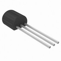
PIN CONFIGURATIONS AND FUNCTION DESCRIPTIONS GND BOTTOM VIEW (Not to Scale) Figure 3. 3-Lead TO-92 Table 4. 3-Lead TO-92 Pin Function Descriptions Pin No. Mnemonic Description 1 V+ Power Supply Input Device ...
Page 6
AD22100 TYPICAL PERFORMANCE CHARACTERISTICS (T0-92 (SOIC 400 FLOW RATE (CFM) Figure 5. Thermal Response vs. Flow Rate 800 1200 Rev Page 250 200 (SOIC) ...
Page 7
... R T Figure 7. Simplified Block Diagram The temperature-dependent resistor, labeled R change in resistance that is nearly linearly proportional to temperature. This resistor is excited with a current source that is proportional to the power supply voltage. The resulting voltage across R is therefore both supply voltage proportional and line- T arly varying with temperature. The remainder of the AD22100 ...
Page 8
... THERMAL ENVIRONMENT EFFECTS The thermal environment in which the AD22100 is used determines two performance traits: the effect of self-heating on accuracy and the response time of the sensor to rapid changes in temperature. In the first case, a rise in the IC junction ) A temperature above the ambient temperature is a function of two ...
Page 9
... Response of the AD22100 output to abrupt changes in ambient temperature can be modeled by a single time constant t expo- nential function. Figure 10 shows the typical response time plots for a few media of interest. 100 ALUMINUM 90 BLOCK MOVING 80 AIR 70 60 STILL AIR TIME (sec) Figure 10. Response Time The time constant t is dependent on θ ...
Page 10
AD22100 OUTLINE DIMENSIONS 0.210 (5.33) 0.170 (4.32) 0.205 (5.21) 0.175 (4.45) 0.135 (3.43) MIN 0.050 (1.27) MAX 0.019 (0.482) 0.055 (1.40) SQ 0.016 (0.407) 0.045 (1.15) 0.105 (2.66) 0.095 (2.42) 0.500 (12.70) MIN SEATING PLANE COMPLIANT TO JEDEC STANDARDS TO-226AA ...
Page 11
... ORDERING GUIDE Models Temperature Range AD22100KT 0°C to +100°C AD22100KR 0°C to +100°C AD22100KR-REEL7 0°C to +100°C 1 AD22100KRZ 0°C to +100°C 1 AD22100KRZ-REEL7 0°C to +100°C AD22100AT –40°C to +85°C AD22100AR –40°C to +85°C AD22100AR-REEL –40°C to +85°C AD22100AR-REEL7 – ...
Page 12
AD22100 NOTES © 2004 Analog Devices, Inc. All rights reserved. Trademarks and regis- tered trademarks are the property of their respective owners. C00673–0–7/04(D) Rev Page ...