2N5911 Vishay, 2N5911 Datasheet - Page 4
2N5911
Manufacturer Part Number
2N5911
Description
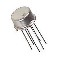
MATCHED N CH JFET PAIR, -25V, TO-78
Manufacturer
Vishay
Specifications of 2N5911
Breakdown Voltage Vbr
-25V
Gate-source Cutoff Voltage Vgs(off) Max
-5V
Power Dissipation Pd
500mW
Operating Temperature Range
-55°C To +150°C
No. Of Pins
6
Continuous Drain Current Id
40mA
Channel Type
N
Configuration
Dual
Gate-source Voltage (max)
25V
Drain-gate Voltage (max)
-25V
Operating Temperature (min)
-55C
Operating Temperature (max)
150C
Operating Temperature Classification
Military
Mounting
Through Hole
Pin Count
7
Package Type
TO-78
Lead Free Status / RoHS Status
Contains lead / RoHS non-compliant


2N5911/5912
Vishay Siliconix
www.vishay.com
8-4
10
10
50
40
30
20
10
0
8
6
4
2
0
8
6
4
2
0
0.1
0
0
Transconductance vs. Gate-Source Voltage
125_C
V
V
Assume V
A
R
GS(off)
T
GS(off)
125_C
V
Circuit Voltage Gain vs. Drain Current
L
A
= –55_C
T
+
+
A
–0.4
–0.4
= –2 V
= –2 V
= –55_C
1 ) R
10 V
V
I
V
D
V
DD
Transfer Characteristics
g
GS(off)
GS
GS
fs
= 15 V, V
I
R
D
– Gate-Source Voltage (V)
25_C
– Gate-Source Voltage (V)
L
L
– Drain Current (mA)
g
= –2 V
os
–0.8
–0.8
DS
1
25_C
= 5 V
–1.2
–1.2
V
GS(off)
V
DS
V
f = 1 kHz
DS
= 10 V
= –5 V
= 10 V
–1.6
–1.6
_
–2
–2
10
200
160
120
30
24
18
12
10
80
40
6
0
8
6
4
2
0
0
1
0
0
Transconductance vs. Gate-Source Voltage
25_C
On-Resistance vs. Drain Current
V
f = 1 kHz
DS
V
–1
–1
125_C
GS(off)
= 10 V
Transfer Characteristics
V
V
V
GS
GS(off)
GS
T
I
A
D
= –5 V
– Gate-Source Voltage (V)
– Gate-Source Voltage (V)
= –55_C
– Drain Current (mA)
= –2 V
–2
–2
–5 V
125_C
10
25_C
V
S-04031—Rev. D, 04-Jun-01
GS(off)
–3
–3
Document Number: 70255
T
A
= –5 V
V
T
= –55_C
A
DS
= 25_C
= 10 V
–4
–4
100
–5
–5
Related parts for 2N5911
Image
Part Number
Description
Manufacturer
Datasheet
Request
R

Part Number:
Description:
357-036-542-201 CARDEDGE 36POS DL .156 BLK LOPRO
Manufacturer:
Vishay
Datasheet:
Part Number:
Description:
357-036-542-201 CARDEDGE 36POS DL .156 BLK LOPRO
Manufacturer:
Vishay
Datasheet:
Part Number:
Description:
357-036-542-201 CARDEDGE 36POS DL .156 BLK LOPRO
Manufacturer:
Vishay
Datasheet:
Part Number:
Description:
357-036-542-201 CARDEDGE 36POS DL .156 BLK LOPRO
Manufacturer:
Vishay
Datasheet:
Part Number:
Description:
357-036-542-201 CARDEDGE 36POS DL .156 BLK LOPRO
Manufacturer:
Vishay
Datasheet:
Part Number:
Description:
357-036-542-201 CARDEDGE 36POS DL .156 BLK LOPRO
Manufacturer:
Vishay
Datasheet:
Part Number:
Description:
357-036-542-201 CARDEDGE 36POS DL .156 BLK LOPRO
Manufacturer:
Vishay
Datasheet:
Part Number:
Description:
357-036-542-201 CARDEDGE 36POS DL .156 BLK LOPRO
Manufacturer:
Vishay
Datasheet:
Part Number:
Description:
357-036-542-201 CARDEDGE 36POS DL .156 BLK LOPRO
Manufacturer:
Vishay
Datasheet:
Part Number:
Description:
357-036-542-201 CARDEDGE 36POS DL .156 BLK LOPRO
Manufacturer:
Vishay
Datasheet:
Part Number:
Description:
357-036-542-201 CARDEDGE 36POS DL .156 BLK LOPRO
Manufacturer:
Vishay
Datasheet:
Part Number:
Description:
357-036-542-201 CARDEDGE 36POS DL .156 BLK LOPRO
Manufacturer:
Vishay
Datasheet:
Part Number:
Description:
357-036-542-201 CARDEDGE 36POS DL .156 BLK LOPRO
Manufacturer:
Vishay
Datasheet:
Part Number:
Description:
357-036-542-201 CARDEDGE 36POS DL .156 BLK LOPRO
Manufacturer:
Vishay
Datasheet:
Part Number:
Description:
357-036-542-201 CARDEDGE 36POS DL .156 BLK LOPRO
Manufacturer:
Vishay
Datasheet: