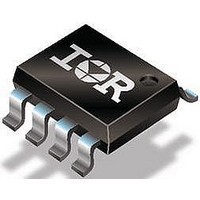
IRF7807ZPBF International Rectifier, IRF7807ZPBF Datasheet - Page 8

IRF7807ZPBF
Manufacturer Part Number
IRF7807ZPBF
Description
N CHANNEL MOSFET, 30V, 11A, SOIC
Manufacturer
International Rectifier
Type
Power MOSFETr
Datasheet
1.IRF7807ZPBF.pdf
(10 pages)
Specifications of IRF7807ZPBF
Transistor Polarity
N Channel
Continuous Drain Current Id
11A
Drain Source Voltage Vds
30V
On Resistance Rds(on)
13.8mohm
Rds(on) Test Voltage Vgs
10V
Threshold Voltage Vgs Typ
1.8V
Configuration
Single Quad Drain Triple Source
Resistance Drain-source Rds (on)
18.2 mOhms
Drain-source Breakdown Voltage
30 V
Gate-source Breakdown Voltage
20 V
Continuous Drain Current
11 A
Power Dissipation
2.5 W
Maximum Operating Temperature
+ 150 C
Mounting Style
SMD/SMT
Package / Case
SOIC-8
Fall Time
3.1 ns
Gate Charge Qg
7.2 nC
Minimum Operating Temperature
- 55 C
Rise Time
6.2 ns
Number Of Elements
1
Polarity
N
Channel Mode
Enhancement
Drain-source On-res
0.0138Ohm
Drain-source On-volt
30V
Gate-source Voltage (max)
±20V
Operating Temp Range
-55C to 150C
Operating Temperature Classification
Military
Mounting
Surface Mount
Pin Count
8
Package Type
SOIC
Lead Free Status / RoHS Status
Lead free / RoHS Compliant
Lead Free Status / RoHS Status
Lead free / RoHS Compliant
Control FET
P
P
Power MOSFET Selection for Non-Isolated DC/DC Converters
loss
8
loss
This can be expanded and approximated by;
= I
+ I ×
+ Q
+
= P
(
⎛
⎜
⎝
(
⎛
⎝
Q
rms
conduction
g
2
oss
× V
2
Q
× R
i
× V
g
gd
g
× f
ds(on )
in
× V
+ P
× f
)
in
)
switching
× f
⎞
⎠
⎞
⎟ + I ×
⎠
+ P
⎛
⎜
⎝
drive
Q
+ P
i
gs 2
g
× V
output
in
× f
⎞
⎟
⎠
Synchronous FET
by;
*dissipated primarily in Q1.
portant characteristic; however, once again the im-
portance of gate charge must not be overlooked since
it impacts three critical areas. Under light load the
MOSFET must still be turned on and off by the con-
trol IC so the gate drive losses become much more
significant. Secondly, the output charge Q
verse recovery charge Q
are transfered to Q1 and increase the dissipation in
that device. Thirdly, gate charge will impact the
MOSFETs’ susceptibility to Cdv/dt turn on.
of the converter and therefore sees transitions be-
tween ground and V
a rate of change of drain voltage dV/dt which is ca-
pacitively coupled to the gate of Q2 and can induce
a voltage spike on the gate that is sufficient to turn
the MOSFET on, resulting in shoot-through current .
The ratio of Q
potential for Cdv/dt turn on.
Figure A: Q
P
P
loss
loss
The power loss equation for Q2 is approximated
For the synchronous MOSFET Q2, R
The drain of Q2 is connected to the switching node
= P
= I
+ Q
+
(
(
⎛
⎜
⎝
conduction
rms
Q
oss
g
2
oss
2
Characteristic
× V
gd
× R
/Q
× V
g
gs1
+ P
ds(on)
× f
in
must be minimized to reduce the
in
. As Q1 turns on and off there is
drive
× f
)
)
rr
⎞
⎠
+ P
both generate losses that
+ Q
output
(
*
rr
× V
www.irf.com
in
ds(on)
× f
oss
is an im-
and re-
)


