IRFB17N50LPBF Vishay, IRFB17N50LPBF Datasheet
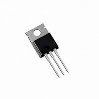
N CHANNEL MOSFET, 500V, 16A, TO-220

IRFB17N50LPBF

Manufacturer Part Number
IRFB17N50LPBF
Description
N CHANNEL MOSFET, 500V, 16A, TO-220
Manufacturer
Vishay
Datasheets

Specifications of IRFB17N50LPBF

Transistor Polarity
N Channel
Continuous Drain Current Id
16A
Drain Source Voltage Vds
500V
On Resistance Rds(on)
320mohm
Rds(on) Test Voltage Vgs
10V
Threshold Voltage Vgs Typ
5V
Fet Type
MOSFET N-Channel, Metal Oxide
Fet Feature
Standard
Rds On (max) @ Id, Vgs
320 mOhm @ 9.9A, 10V
Drain To Source Voltage (vdss)
500V
Current - Continuous Drain (id) @ 25° C
16A
Vgs(th) (max) @ Id
5V @ 250µA
Gate Charge (qg) @ Vgs
130nC @ 10V
Input Capacitance (ciss) @ Vds
2760pF @ 25V
Power - Max
220W
Mounting Type
Through Hole
Package / Case
TO-220-3 (Straight Leads)
Minimum Operating Temperature
- 55 C
Configuration
Single
Resistance Drain-source Rds (on)
0.32 Ohm @ 10 V
Drain-source Breakdown Voltage
500 V
Gate-source Breakdown Voltage
+/- 30 V
Continuous Drain Current
16 A
Power Dissipation
220000 mW
Maximum Operating Temperature
+ 150 C
Mounting Style
Through Hole
Lead Free Status / RoHS Status
Lead free / RoHS Compliant
Lead Free Status / RoHS Status
Lead free / RoHS Compliant, Lead free / RoHS Compliant
Other names
*IRFB17N50LPBF

Available stocks

Company
Part Number
Manufacturer
Quantity
Price
Part Number:
IRFB17N50LPBF
Manufacturer:
ST
Quantity:
6 000
Company:
Part Number:
IRFB17N50LPBF
Quantity:
6 000
Company:
Part Number:
IRFB17N50LPBF
Quantity:
12 007
Company:
Part Number:
IRFB17N50LPBF
Quantity:
70 000
Diode Characteristics
Benefits
Document Number: 91098
l
l
l
l
l
l
l
l
l
l
l
Typical SMPS Topologies
l
Absolute Maximum Ratings
Applications
I
I
I
P
V
dv/dt
T
T
Symbol
I
I
V
t
Q
I
t
D
D
DM
S
SM
rr
RRM
on
D
GS
J
STG
SD
rr
and Current
@ T
@ T
Switch Mode Power Supply (SMPS)
Uninterruptible Power Supply
High Speed Power Switching
ZVS and High Frequency Circuit
PWM Inverters
Lead-Free
Low Gate Charge Qg results in Simple Drive Requirement
Improved Gate, Avalanche and Dynamic dv/dt Ruggedness
Fully Characterized Capacitance and Avalanche Voltage
Low Trr and Soft Diode Recovery
High Performance Optimised Anti-parallel Diode
@T
Bridge Converters
C
C
C
= 25°C
= 100°C
= 25°C
Continuous Source Current
(Body Diode)
Pulsed Source Current
(Body Diode) 
Diode Forward Voltage
Reverse Recovery Current
Forward Turn-On Time
Reverse Recovery Time
Reverse Recovery Charge
Continuous Drain Current, V
Pulsed Drain Current 
Power Dissipation
Linear Derating Factor
Gate-to-Source Voltage
Peak Diode Recovery dv/dt ƒ
Operating Junction and
Storage Temperature Range
Soldering Temperature, for 10 seconds
Mounting Torque, 6-32 or M3 screw
(1.6mm from case )
Parameter
Parameter
l
All Zero Voltage Switching
SMPS MOSFET
GS
GS
@ 10V
@ 10V
Min. Typ. Max. Units
–––
–––
–––
–––
–––
–––
–––
–––
Intrinsic turn-on time is negligible (turn-on is dominated by L
–––
–––
–––
170
220
470
810 1210
7.3
250
330
710
V
500V
1.5
16
64
11
IRFB17N50LPbF
DSS
nC
ns
V
A
-55 to + 150
HEXFET
MOSFET symbol
showing the
integral reverse
p-n junction diode.
T
T
T
T
T
Max.
220
± 30
300
1.8
J
J
J
J
J
16
11
64
13
10
= 25°C, I
= 25°C
= 125°C
= 25°C
= 125°C
R
DS(on)
0.28Ω
®
S
Conditions
= 16A, V
Power MOSFET
typ.
TO-220AB
di/dt = 100A/µs „
I
F
= 16A
GS
www.vishay.com
PD - 95123
lbft.in(N.m)
= 0V „
G
Units
W/°C
V/ns
W
°C
A
V
S
16A
3/18/04
+L
I
D
D
S
D
)
1

Related parts for IRFB17N50LPBF

IRFB17N50LPBF Summary of contents

Page 1

... Reverse Recovery Time rr Q Reverse Recovery Charge rr I Reverse Recovery Current RRM t Forward Turn-On Time on Typical SMPS Topologies Bridge Converters l Document Number: 91098 IRFB17N50LPbF SMPS MOSFET V DSS 500V @ 10V GS @ 10V GS Min. Typ. Max. Units 16 ––– ––– 64 ––– ...

Page 2

... DS pF ƒ = 1.0MHz 1.0V, ƒ = 1.0MHz 0V 400V, ƒ = 1.0MHz 0V 400V … Typ. Max. Units ––– 390 ––– 16 ––– 22 Typ. Max. Units ––– 0.56 0.50 ––– °C/W ––– 62 www.vishay.com ...

Page 3

... Fig 4. Normalized On-Resistance VGS 15V 12V 10V 8.0V 7.0V 6.0V 5.5V 5.0V 20µs PULSE WIDTH Tj = 150° Drain-to-Source Voltage (V) 16A 100 120 140 160 ° Junction Temperature ( C) J Vs. Temperature www.vishay.com 100 10V 3 ...

Page 4

... Fig 8. Maximum Safe Operating Area 16A V = 400V 250V 100V 120 Q , Total Gate Charge (nC) G Gate-to-Source Voltage OPERATION IN THIS AREA LIMITED BY R DS(on) 10us 100us 1ms 10ms = 25 C ° ° = 150 C 100 1000 V , Drain-to-Source Voltage (V) DS www.vishay.com 150 10000 4 ...

Page 5

... Fig 11. Maximum Effective Transient Thermal Impedance, Junction-to-Case Document Number: 91098 Fig 10a. Switching Time Test Circuit V DS 90% 125 150 ° 10 d(on) Fig 10b. Switching Time Waveforms 0.001 0. Rectangular Pulse Duration (sec ≤ 1 ≤ 0 d(off Notes: 1. Duty factor Peak thJC C 0.1 www.vishay.com 1 5 ...

Page 6

... Fig 13a. Gate Charge Test Circuit Document Number: 91098 I D TOP 7A 10A BOTTOM 16A R G Fig 12c. Unclamped Inductive Test Circuit 125 150 ° Fig 12d. Unclamped Inductive Waveforms Fig 13b. Basic Gate Charge Waveform 15V DRIVER D.U 20V 0.01 Ω (BR)DSS Charge www.vishay.com A 6 ...

Page 7

... Voltage Inductor Curent * Fig 14. For N-Channel HEXFET Document Number: 91098 + • • ƒ • - „ • • • • P.W. Period D = Period Body Diode Forward Current di/dt Diode Recovery dv/dt Body Diode Forward Drop Ripple ≤ 5% ® Power MOSFETs + - * V =10V www.vishay.com 7 ...

Page 8

... LEAD ASSIGNMENTS LEAD ASSIGNMENTS HEXFET IGBTs, CoPACK 1 - GATE 2 - DRAIN 1- GATE 1- GATE 2- DRAIN 3 - SOURCE 2- COLLECTOR 3- SOURCE 3- EMITTER 4 - DRAIN 4- DRAIN 4- COLLECTOR 0.55 (.022) 3X 0.46 (.018) 2.92 (.115) 2.64 (.104) PAR DAT E CODE 1997 INE C TAC Fax: (310) 252-7903 03/04 www.vishay.com 8 ...

Page 9

... Except as provided in Vishay's terms and conditions of sale for such products, Vishay assumes no liability whatsoever, and disclaims any express or implied warranty, relating to sale and/or use of Vishay products including liability or warranties relating to fitness for a particular purpose, merchantability, or infringement of any patent, copyright, or other intellectual property right. ...

Related keywords