2N6661 Vishay, 2N6661 Datasheet - Page 2
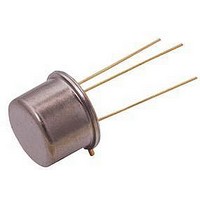
2N6661
Manufacturer Part Number
2N6661
Description
N CH MOSFET, 90V, 900mA, TO-205AD
Manufacturer
Vishay
Type
Power MOSFETr
Datasheet
1.2N6661.pdf
(5 pages)
Specifications of 2N6661
Transistor Polarity
N Channel
Continuous Drain Current Id
860mA
Drain Source Voltage Vds
90V
On Resistance Rds(on)
4ohm
Rds(on) Test Voltage Vgs
10V
Threshold Voltage Vgs Typ
1.6V
Configuration
Single
Resistance Drain-source Rds (on)
4 Ohms
Drain-source Breakdown Voltage
90 V
Gate-source Breakdown Voltage
+/- 20 V
Continuous Drain Current
0.9 A
Power Dissipation
6.25 W
Maximum Operating Temperature
+ 150 C
Mounting Style
Stud
Package / Case
TO-205AD
Minimum Operating Temperature
- 55 C
Number Of Elements
1
Polarity
N
Channel Mode
Enhancement
Drain-source On-res
4Ohm
Drain-source On-volt
90V
Gate-source Voltage (max)
±20V
Output Power (max)
Not RequiredW
Frequency (max)
Not RequiredMHz
Noise Figure
Not RequireddB
Power Gain
Not RequireddB
Drain Efficiency
Not Required%
Operating Temp Range
-55C to 150C
Operating Temperature Classification
Military
Mounting
Through Hole
Pin Count
3
Package Type
TO-205AD
Lead Free Status / RoHS Status
Contains lead / RoHS non-compliant
Available stocks
Company
Part Number
Manufacturer
Quantity
Price

Part Number:
2N6661
Manufacturer:
SSI
Quantity:
20 000


Notes
a.
b.
c.
d.
www.vishay.com
11-2
2N6661/VN88AFD
Vishay Siliconix
Static
Drain-Source Breakdown Voltage
Gate-Threshold Voltage
Gate-Body Leakage
Zero Gate Voltage Drain Current
On-State Drain Current
Drain-Source On-Resistance
Forward Transconductance
Diode Forward Voltage
Dynamic
Input Capacitance
Output Capacitance
Reverse Transfer Capacitance
Drain-Source Capacitance
Switching
Turn-On Time
Turn-Off Time
For DESIGN AID ONLY, not subject to production testing.
Pulse test: PW v300 ms duty cycle v2%.
Switching time is essentially independent of operating temperature.
This parameter not registered with JEDEC.
c
Parameter
b
b
b
_
Symbol
V
V
r
(BR)DSS
I
DS(on)
I
I
C
D(on)
V
C
t
GS(th)
C
GSS
C
t
DSS
OFF
g
ON
SD
oss
iss
rss
ds
fs
V
DS
V
V
V
= 0.8 x V
V
I
V
V
V
I
V
V
Test Conditions
V
V
DS
D
DS
DS
V
S
V
DD
DS
DS
DS
DS
DS
DS
GS
GS
^
^ 1 A, V
GS
= 0.86 A, V
= 0 V, V
= 15 V, V
= 10 V, V
= 25 V, R
= 90 V, V
= 80 V, V
= 24 V, V
= 24 V, V
= V
= 10 V, I
= 0 V, I
= 5 V, I
= 10 V, I
R
f = 1 MHz
G
GS
(BR)DSS
= 25 W
, I
GS
GEN
D
D
D
D
GS
GS
GS
GS
GS
GS
GS
= 10 mA
D
L
= 0.3 A
= "15 V
= 1 mA
= 0.5 A
= 23 W
, V
=
= 10 V
= 10 V
= 10 V
= 0 V
= 0 V
= 0 V
= 0 V
= 0 V
1
T
T
T
T
T
GS
J
J
J
J
A
J
= 125_C
= –55_C
= 125_C
= 125_C
= 0 V
= 125_C
d
Typ
125
350
1.6
1.8
1.3
1.8
1.8
3.8
3.6
6.7
0.9
35
15
30
2
6
8
a
Min
170
0.8
1.5
90
2N6661
Max
"100
"500
500
5.3
10
50
40
10
40
10
10
2
4
9
Limits
S-04279—Rev. C, 16-Jul-01
Document Number: 70224
Min
170
0.8
1.5
80
VN88AFD
"100
"500
Max
500
2.5
5.6
10
50
40
10
15
15
1
4
8
VNDQ09
Unit
mS
nA
m
mA
pF
ns
W
V
A
V
Related parts for 2N6661
Image
Part Number
Description
Manufacturer
Datasheet
Request
R

Part Number:
Description:
357-036-542-201 CARDEDGE 36POS DL .156 BLK LOPRO
Manufacturer:
Vishay
Datasheet:
Part Number:
Description:
357-036-542-201 CARDEDGE 36POS DL .156 BLK LOPRO
Manufacturer:
Vishay
Datasheet:
Part Number:
Description:
357-036-542-201 CARDEDGE 36POS DL .156 BLK LOPRO
Manufacturer:
Vishay
Datasheet:
Part Number:
Description:
357-036-542-201 CARDEDGE 36POS DL .156 BLK LOPRO
Manufacturer:
Vishay
Datasheet:
Part Number:
Description:
357-036-542-201 CARDEDGE 36POS DL .156 BLK LOPRO
Manufacturer:
Vishay
Datasheet:
Part Number:
Description:
357-036-542-201 CARDEDGE 36POS DL .156 BLK LOPRO
Manufacturer:
Vishay
Datasheet:
Part Number:
Description:
357-036-542-201 CARDEDGE 36POS DL .156 BLK LOPRO
Manufacturer:
Vishay
Datasheet:
Part Number:
Description:
357-036-542-201 CARDEDGE 36POS DL .156 BLK LOPRO
Manufacturer:
Vishay
Datasheet:
Part Number:
Description:
357-036-542-201 CARDEDGE 36POS DL .156 BLK LOPRO
Manufacturer:
Vishay
Datasheet:
Part Number:
Description:
357-036-542-201 CARDEDGE 36POS DL .156 BLK LOPRO
Manufacturer:
Vishay
Datasheet:
Part Number:
Description:
357-036-542-201 CARDEDGE 36POS DL .156 BLK LOPRO
Manufacturer:
Vishay
Datasheet:
Part Number:
Description:
357-036-542-201 CARDEDGE 36POS DL .156 BLK LOPRO
Manufacturer:
Vishay
Datasheet:
Part Number:
Description:
357-036-542-201 CARDEDGE 36POS DL .156 BLK LOPRO
Manufacturer:
Vishay
Datasheet:
Part Number:
Description:
357-036-542-201 CARDEDGE 36POS DL .156 BLK LOPRO
Manufacturer:
Vishay
Datasheet:
Part Number:
Description:
357-036-542-201 CARDEDGE 36POS DL .156 BLK LOPRO
Manufacturer:
Vishay
Datasheet: