SI8409DB-T1-E1 Vishay, SI8409DB-T1-E1 Datasheet

P CH MOSFET, -30V, 6.3A, MICRO FOOT

SI8409DB-T1-E1

Manufacturer Part Number
SI8409DB-T1-E1
Description
P CH MOSFET, -30V, 6.3A, MICRO FOOT
Manufacturer
Vishay
Series
TrenchFET®r
Datasheet

Specifications of SI8409DB-T1-E1

Transistor Polarity
P Channel
Continuous Drain Current Id
-6.3A
Drain Source Voltage Vds
-30V
On Resistance Rds(on)
65mohm
Rds(on) Test Voltage Vgs
12V
Threshold Voltage Vgs Typ
1.4V
Fet Type
MOSFET P-Channel, Metal Oxide
Fet Feature
Logic Level Gate
Rds On (max) @ Id, Vgs
46 mOhm @ 1A, 4.5V
Drain To Source Voltage (vdss)
30V
Current - Continuous Drain (id) @ 25° C
4.6A
Vgs(th) (max) @ Id
1.4V @ 250µA
Gate Charge (qg) @ Vgs
26nC @ 4.5V
Power - Max
1.47W
Mounting Type
Surface Mount
Package / Case
4-MICRO FOOT®CSP
Minimum Operating Temperature
- 55 C
Configuration
Single Dual Drain
Resistance Drain-source Rds (on)
0.046 Ohm @ 4.5 V
Forward Transconductance Gfs (max / Min)
6.4 S
Drain-source Breakdown Voltage
30 V
Gate-source Breakdown Voltage
+/- 12 V
Continuous Drain Current
4.6 A
Power Dissipation
1470 mW
Maximum Operating Temperature
+ 150 C
Mounting Style
SMD/SMT
Lead Free Status / RoHS Status
Lead free / RoHS Compliant
Lead Free Status / RoHS Status
Lead free / RoHS Compliant, Lead free / RoHS Compliant
Other names
SI8409DB-T1-E1TR

Available stocks

Company
Part Number
Manufacturer
Quantity
Price
Part Number:
SI8409DB-T1-E1
Manufacturer:
Freescale
Quantity:
37
Part Number:
SI8409DB-T1-E1
Manufacturer:
VISHAY
Quantity:
8 000
Company:
Part Number:
SI8409DB-T1-E1
Quantity:
300
Notes:
a. Surface Mounted on 1" x 1" FR4 board.
b. Refer to IPC/JEDEC (J-STD-020C), no manual or hand soldering.
Document Number: 73111
S-82118-Rev. B, 08-Sep-08
PRODUCT SUMMARY
ABSOLUTE MAXIMUM RATINGS T
Parameter
Drain-Source Voltage
Gate-Source Voltage
Continuous Drain Current (T
Pulsed Drain Current
Continuous Source Current (Diode Conduction)
Maximum Power Dissipation
Operating Junction and Storage Temperature Range
Package Reflow Conditions
THERMAL RESISTANCE RATINGS
Parameter
Maximum Junction-to-Ambient
Maximum Junction-to-Foot (drain)
V
DS
- 30
(V)
3
4
Ordering Information: Si8409DB-T1-E1 (Lead (Pb)-free)
Bump Side View
D
S
Device Marking: 8409
0.046 at V
0.065 at V
R
DS(on)
D
G
GS
GS
MICRO FOOT
= - 4.5 V
= - 2.5 V
(Ω)
b
2
1
J
a
xxx = Date/Lot Traceability Code
= 150 °C)
a
P-Channel 30-V (D-S) MOSFET
Backside View
a
8409
I
xxx
D
- 6.3
- 5.3
(A)
a
A
Q
= 25 °C, unless otherwise noted
IR/Convection
g
Steady State
Steady State
T
T
T
T
(Typ.)
17
A
A
A
A
t ≤ 5 s
= 25 °C
= 70 °C
= 25 °C
= 70 °C
FEATURES
APPLICATIONS
• TrenchFET
• MICRO FOOT
• Pin Compatible to Si8401DB
• Load Switch, Battery Switch, and PA Switch for Portable
Symbol
Symbol
T
R
R
J
Reduces Footprint Area Profile (0.62 mm) and
On-Resistance Per Footprint Area
Devices
V
V
I
P
, T
I
DM
thJA
thJF
I
DS
GS
D
S
D
G
stg
P-Channel MOSFET
®
S
D
Power MOSFET
Typical
®
- 6.3
- 5.1
- 2.5
2.77
1.77
5 s
35
72
16
Chipscale Packaging
- 55 to 150
± 12
- 30
- 25
260
Steady State
Maximum
- 4.6
- 3.7
- 1.3
1.47
0.94
45
85
20
Vishay Siliconix
Si8409DB
www.vishay.com
°C/W
Unit
Unit
°C
W
V
A
RoHS
COMPLIANT
1

Related parts for SI8409DB-T1-E1

SI8409DB-T1-E1 Summary of contents

Page 1

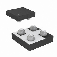
... Bump Side View Backside View Device Marking: 8409 xxx = Date/Lot Traceability Code Ordering Information: Si8409DB-T1-E1 (Lead (Pb)-free) ABSOLUTE MAXIMUM RATINGS T Parameter Drain-Source Voltage Gate-Source Voltage a Continuous Drain Current (T = 150 °C) J Pulsed Drain Current Continuous Source Current (Diode Conduction) a Maximum Power Dissipation ...

Page 2

... Si8409DB Vishay Siliconix SPECIFICATIONS °C, unless otherwise noted J Parameter Static Gate Threshold Voltage Gate-Body Leakage Zero Gate Voltage Drain Current a On-State Drain Current a Drain-Source On-State Resistance a Forward Transconductance a Diode Forward Voltage b Dynamic Total Gate Charge Gate-Source Charge Gate-Drain Charge Gate Resistance ...

Page 3

... 0.0 0.2 0.4 0.6 0 Source-to-Drain Voltage (V) SD Source-Drain Diode Forward Voltage Document Number: 73111 S-82118-Rev. B, 08-Sep- 4 °C J 1.0 1.2 1.4 1.6 Si8409DB Vishay Siliconix 1500 1200 C iss 900 600 C oss 300 C rss Drain-to-Source Voltage (V) DS Capacitance 1 1.4 1 ...

Page 4

... Si8409DB Vishay Siliconix TYPICAL CHARACTERISTICS 25 °C, unless otherwise noted 0 250 µA 0.5 D 0.4 0.3 0.2 0.1 0.0 - 0 Temperature (°C) J Threshold Voltage 2 1 Duty Cycle = 0.5 0.2 0.1 0.1 0.05 0.02 Single Pulse 0. www.vishay.com 4 75 100 125 150 100 * Limited R DS(on) ...

Page 5

... TYPICAL CHARACTERISTICS 25 °C, unless otherwise noted 2 1 Duty Cycle = 0.5 0.2 0.1 0.1 0.05 0.02 Single Pulse 0. Document Number: 73111 S-82118-Rev. B, 08-Sep- Square Wave Pulse Duration (s) Normalized Thermal Transient Impedance, Junction-to-Foot Si8409DB Vishay Siliconix - www.vishay.com 10 5 ...

Page 6

... Si8409DB Vishay Siliconix PACKAGE OUTLINE MICRO FOOT: 4-BUMP ( 0.8 mm PITCH Recommended Land 8409 XXX Mark on Backside of Die Notes (Unless Otherwise Specified): 1. Laser mark on the silicon die back, coated with a thin metal. 2. Bumps are 95.5/3.8/0.7 Sn/Ag/Cu. 3. Non-solder mask defined copper landing pad. ...

Page 7

... Vishay product could result in personal injury or death. Customers using or selling Vishay products not expressly indicated for use in such applications their own risk and agree to fully indemnify and hold Vishay and its distributors harmless from and against any and all claims, liabilities, expenses and damages arising or resulting in connection with such use or sale, including attorneys fees, even if such claim alleges that Vishay or its distributor was negligent regarding the design or manufacture of the part ...

Related keywords