SI8409DB-T1-E1 Vishay, SI8409DB-T1-E1 Datasheet - Page 6
SI8409DB-T1-E1
Manufacturer Part Number
SI8409DB-T1-E1
Description
P CH MOSFET, -30V, 6.3A, MICRO FOOT
Manufacturer
Vishay
Series
TrenchFET®r
Datasheet
1.SI8409DB-T1-E1.pdf
(7 pages)
Specifications of SI8409DB-T1-E1
Transistor Polarity
P Channel
Continuous Drain Current Id
-6.3A
Drain Source Voltage Vds
-30V
On Resistance Rds(on)
65mohm
Rds(on) Test Voltage Vgs
12V
Threshold Voltage Vgs Typ
1.4V
Fet Type
MOSFET P-Channel, Metal Oxide
Fet Feature
Logic Level Gate
Rds On (max) @ Id, Vgs
46 mOhm @ 1A, 4.5V
Drain To Source Voltage (vdss)
30V
Current - Continuous Drain (id) @ 25° C
4.6A
Vgs(th) (max) @ Id
1.4V @ 250µA
Gate Charge (qg) @ Vgs
26nC @ 4.5V
Power - Max
1.47W
Mounting Type
Surface Mount
Package / Case
4-MICRO FOOT®CSP
Minimum Operating Temperature
- 55 C
Configuration
Single Dual Drain
Resistance Drain-source Rds (on)
0.046 Ohm @ 4.5 V
Forward Transconductance Gfs (max / Min)
6.4 S
Drain-source Breakdown Voltage
30 V
Gate-source Breakdown Voltage
+/- 12 V
Continuous Drain Current
4.6 A
Power Dissipation
1470 mW
Maximum Operating Temperature
+ 150 C
Mounting Style
SMD/SMT
Lead Free Status / RoHS Status
Lead free / RoHS Compliant
Lead Free Status / RoHS Status
Lead free / RoHS Compliant, Lead free / RoHS Compliant
Other names
SI8409DB-T1-E1TR
Available stocks
Company
Part Number
Manufacturer
Quantity
Price
Company:

Part Number:
SI8409DB-T1-E1
Manufacturer:
Freescale
Quantity:
37


Si8409DB
Vishay Siliconix
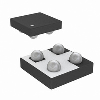
PACKAGE OUTLINE
MICRO FOOT: 4-BUMP (2 x 2, 0.8 mm PITCH)
Notes (Unless Otherwise Specified):
1. Laser mark on the silicon die back, coated with a thin metal.
2. Bumps are 95.5/3.8/0.7 Sn/Ag/Cu.
3. Non-solder mask defined copper landing pad.
4. The flat side of wafers is oriented at the bottom.
Notes:
a. Use millimeters as the primary measurement.
Vishay Siliconix maintains worldwide manufacturing capability. Products may be manufactured at one of several qualified locations. Reliability data for Silicon
Technology and Package Reliability represent a composite of all qualified locations. For related documents such as package/tape drawings, part marking, and
reliability data, see http://www.vishay.com/ppg?73111.
www.vishay.com
6
Dim.
A
A
A
D
E
S
b
e
1
2
e
Recommended Land
Mark on Backside of Die
8409
XXX
0.600
0.260
0.340
0.370
1.520
1.520
0.750
0.370
e
Min.
Millimeters
4 x φ 0.30
Note 3
Solder Mask φ
a
b Diamerter
0.650
0.290
0.360
0.410
1.600
1.600
0.850
0.380
Max.
A
∼
0.31
A
A
∼
2
1
0.40
E
Silicon
e
D
0.0236
0.0102
0.0134
0.0146
0.0598
0.0598
0.0295
0.0146
Min.
S
Inches
Bump Note 2
S-82118-Rev. B, 08-Sep-08
Document Number: 73111
S
e
0.0256
0.0114
0.0142
0.0161
0.0630
0.0630
0.0335
0.0150
Max.
Related parts for SI8409DB-T1-E1
Image
Part Number
Description
Manufacturer
Datasheet
Request
R

Part Number:
Description:
P-channel 30-v D-s Mosfet
Manufacturer:
Vishay
Datasheet:
Part Number:
Description:
357-036-542-201 CARDEDGE 36POS DL .156 BLK LOPRO
Manufacturer:
Vishay
Datasheet:
Part Number:
Description:
357-036-542-201 CARDEDGE 36POS DL .156 BLK LOPRO
Manufacturer:
Vishay
Datasheet:
Part Number:
Description:
357-036-542-201 CARDEDGE 36POS DL .156 BLK LOPRO
Manufacturer:
Vishay
Datasheet:
Part Number:
Description:
357-036-542-201 CARDEDGE 36POS DL .156 BLK LOPRO
Manufacturer:
Vishay
Datasheet:
Part Number:
Description:
357-036-542-201 CARDEDGE 36POS DL .156 BLK LOPRO
Manufacturer:
Vishay
Datasheet:
Part Number:
Description:
357-036-542-201 CARDEDGE 36POS DL .156 BLK LOPRO
Manufacturer:
Vishay
Datasheet:
Part Number:
Description:
357-036-542-201 CARDEDGE 36POS DL .156 BLK LOPRO
Manufacturer:
Vishay
Datasheet:
Part Number:
Description:
357-036-542-201 CARDEDGE 36POS DL .156 BLK LOPRO
Manufacturer:
Vishay
Datasheet:
Part Number:
Description:
357-036-542-201 CARDEDGE 36POS DL .156 BLK LOPRO
Manufacturer:
Vishay
Datasheet:
Part Number:
Description:
357-036-542-201 CARDEDGE 36POS DL .156 BLK LOPRO
Manufacturer:
Vishay
Datasheet:
Part Number:
Description:
357-036-542-201 CARDEDGE 36POS DL .156 BLK LOPRO
Manufacturer:
Vishay
Datasheet:
Part Number:
Description:
357-036-542-201 CARDEDGE 36POS DL .156 BLK LOPRO
Manufacturer:
Vishay
Datasheet:
Part Number:
Description:
357-036-542-201 CARDEDGE 36POS DL .156 BLK LOPRO
Manufacturer:
Vishay
Datasheet:
Part Number:
Description:
357-036-542-201 CARDEDGE 36POS DL .156 BLK LOPRO
Manufacturer:
Vishay
Datasheet: