PG12864LRF-NRA-H-Q POWERTIP, PG12864LRF-NRA-H-Q Datasheet
PG12864LRF-NRA-H-Q
Specifications of PG12864LRF-NRA-H-Q


Related parts for PG12864LRF-NRA-H-Q

PG12864LRF-NRA-H-Q Summary of contents
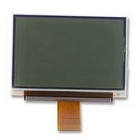
Page 1
... POWERTIP TECH. CORP. DISPLAY DEVICES FOR BETTER ELECTRONIC DESIGN Customer Model Type Sample Code Mass Production Code Edition Customer Sign 【產品規格書】 LCD Module PG12864LRF-NRA-H-S0 0 Sales Sign Approved By Prepared By NO.PT-R-003-4 ...
Page 2
... Mechanical Specifications 1.3 Absolute Maximum Ratings 1.4 DC Electrical Characteristics 1.5 Optical Characteristics 1.6 Backlight Characteristics 2. MODULE STRUCTURE 2.1 Counter Drawing 2.2 Interface Pin Description 2.3 Timing Characteristics 2.4 Display Command POWERTIP TECHNOLOGY CORPORATION DISPLAY DEVICES FOR BETTER ELECTRONIC DESIGN CONTENTS ...
Page 3
... Symbol Conditions Min OPR T - STG Symbol Condition =3. POWERTIP TECHNOLOGY CORPORATION DISPLAY DEVICES FOR BETTER ELECTRONIC DESIGN Max. Unit -0.3 6 °C -20 70 °C - %RH V =0, V =1.8~5.5V, Ta=-30~85° Min. Typ. Max. 1.8 3.3 5 0.6 ...
Page 4
... Symbol Viewing angle Contrast Response time(rise) Response time(fall) Parameter Symbol Driving V OP voltage Note 1: Definition of angles θ and ∅ POWERTIP TECHNOLOGY CORPORATION DISPLAY DEVICES FOR BETTER ELECTRONIC DESIGN Conditions Min. θ C>2.0,∅=0° 40° θ=5°, ∅ C 0° θ=5°, ∅ ...
Page 5
... B2 unselected dot V OPR t : Response time (rise) r POWERTIP TECHNOLOGY CORPORATION DISPLAY DEVICES FOR BETTER ELECTRONIC DESIGN θ1 θ2 viewing angle θ (∅ fixed) Optimum viewing angle with the naked eye and viewing angle θ at Cmax. Above are not always the same ...
Page 6
... Reverse voltage Power dissipation Operating Temperature Storage temperature Electrical Ratings •. Item Symbol Forward voltage Reverse current Luminous intensity (without LCD) Luminous intensity (without LCD) Wavelength Color POWERTIP TECHNOLOGY CORPORATION DISPLAY DEVICES FOR BETTER ELECTRONIC DESIGN Symbol Conditions Min =25° =25° ...
Page 7
... Be sure to set this pin at “L” after completion of transfer or at not accessing. Used as serial data input pin when serial interface is selected. LED Backlight (+3.3V, 40mA) LED Backlight (-) POWERTIP TECHNOLOGY CORPORATION DISPLAY DEVICES FOR BETTER ELECTRONIC DESIGN Function Read/Write Serial clock RS S0-D7 RDB,WRB ...
Page 8
... Timing Characteristics 2.3.1 system Bus Read/Write Timing (80 Family MPU) ․ Read timing ․ Write timing ․ (MPU timing characteristics) POWERTIP TECHNOLOGY CORPORATION DISPLAY DEVICES FOR BETTER ELECTRONIC DESIGN ...
Page 9
... Symbol Mesauring condition MIN MAX Unit t AH8 t AS8 t CYC8 t RDW8 t WRW8 t DS8 t DH8 t C =15pF RDD8 L t RDH8 POWERTIP TECHNOLOGY CORPORATION DISPLAY DEVICES FOR BETTER ELECTRONIC DESIGN Applicable pin 60 ns CSB 450 ns RDB 270 ns WRB 100 ns 100 220 All of above pins (V =2.4 to 2.7V,Ta=-30 to +85℃ ...
Page 10
... CSH Symbol Mesauring condition MIN MAX Unit t CYCS t SHW t SLW t ASS t AHS t DSS t DHS t CSS t CSH POWERTIP TECHNOLOGY CORPORATION DISPLAY DEVICES FOR BETTER ELECTRONIC DESIGN (VDD=2.4~5.5V,Ta=-30 to +85℃) Applicable pin 1000 ns SCL 400 ns 400 400 SDA 400 CSB All of above pins (VDD=1.8~2.4V,Ta=-30 to +85℃ ...
Page 11
... AX3 AX2 Data Codes (7-3~7-16 Display RAM write data Display RAM read data AX3 AY3 ※ POWERTIP TECHNOLOGY CORPORATION DISPLAY DEVICES FOR BETTER ELECTRONIC DESIGN D1 D0 AX1 AX0 AX2 AX1 AX0 AY2 AY1 AY0 AY6 AY5 AY4 ...
Page 12
... When the n line alternated drive command is OFF (NLIN=”0”), alternated drive waveform which reverses by frame cycle is generated. LA5 LA4 LA3 DISPLAY DEVICES FOR BETTER ELECTRONIC DESIGN LY3 ※ LA2 LA1 LA0 LINE ADDRESS ※ LA2 LA1 LA0 LINE ADDRESS POWERTIP TECHNOLOGY CORPORATION LY2 LY1 LY0 LA5 LA4 ※ ※ ...
Page 13
... Regardless of the data of the Graphic Display RAM, the Graphic Display are on. This command has priority over display normal/reverse commands. SEGON=”0”:display OFF SEGON=”1”:display ON DISPLAY DEVICES FOR BETTER ELECTRONIC DESIGN SHIFT The terminals are specified VSS level. POWERTIP TECHNOLOGY CORPORATION SEGMENT ALLON ON/OFF ...
Page 14
... LH155BA5 REV INTERNAL ACCESS D7~D0 X ADDRESS D0(LSB) NH D7(MSB) D0(LSB) 0FH-NH D7(MSB) INTERNAL ACCESS POWERTIP TECHNOLOGY CORPORATION ※ NLIN SWAP REF DDRRESPONDING SEG OUTPUT D7-D0 (LSB) SEG(8*NH) Output (MSB) SEG(8*NH+7) Output (MSB) SEG(8*(0F-NH)+7) Output (LSB) SEG(8*(0F-NH)) Output DDRRESPONDING ...
Page 15
... D0(LSB) 01H D3(MSB) D0(LSB) 00H D7(MSB) D0(LSB) 01H D3(MSB) SWAP=”0” ※ POWERTIP TECHNOLOGY CORPORATION SEG OUTPUT D7-D0 D0(LSB) D7->D0 D7(MSB) SEGS0->SEGS7 D0(LSB) D0~D3 D3(MSB) SEGS8->SEGS11 D0(LSB) D0->D7 D7(MSB) SEGS0->SEGS7 D0(LSB) D0->D3 D3(MSB) SEGS8->SEGS11 SWAP=”1” ...
Page 16
... This is effective when subsequently writing and reading the successive address area. <2> This is effective in the case that after reading and writing the successive address area every address, the read data are modified to write. POWERTIP TECHNOLOGY CORPORATION DISPLAY DEVICES FOR BETTER ELECTRONIC DESIGN REFERENCE < ...
Page 17
... At REF=”0” (normal output) 00H 0FH (X address) vary in the above loops. ‧ At REF=”1” (reverse output) 0FH 00H (X address) vary in the above loops. POWERTIP TECHNOLOGY CORPORATION DISPLAY DEVICES FOR BETTER ELECTRONIC DESIGN REFERENCE 0FH 00H 00H 3FH 00H 3FH (Y address) ...
Page 18
... The LCD drive voltage V0 output from the built-in power circuit can be controlled and the display controlled and the display tone on the LCD can be also controlled. The LCD drive V0 takes one out of 16 voltage values by setting 4 bit data register. DISPLAY DEVICES FOR BETTER ELECTRONIC DESIGN BIAS MSS POWERTIP TECHNOLOGY CORPORATION HALT PON ACL …… LSB ...
Page 19
... Duty Command Select Duty ratic below.. DUTY DISPLAY DEVICES FOR BETTER ELECTRONIC DESIGN V0/SV0 Smaller Typ Larger SEGPON DU1 BOOST VOLTAGE LEVEL 4 TIMES 3 TIMES 2 TIMES PROHIBITION DUTY RATIO 1/64 1/48 1/32 1/16 POWERTIP TECHNOLOGY CORPORATION EXA ICON ※ DU0 BS1 D0 BS0 ...
Page 20
... The LH155BA allows parallel data transfer by connecting the data bus to an 8-bit ※ RA3 ※ ※ ※ RS RDB WRB CSB RS RDB WRB CSB POWERTIP TECHNOLOGY CORPORATION DISPLAY DEVICES FOR BETTER ELECTRONIC DESIGN ※ ※ RA2 RA1 RA0 Internal register read data M86 SDA SCL M86 - - SDA SCL Data - ...
Page 21
... DISPLAY DEVICES FOR BETTER ELECTRONIC DESIGN CSB RS CSB RS 80-family WRB RDB POWERTIP TECHNOLOGY CORPORATION RDB WRB Data RDB WRB FUNCTION 1 Read internal register 0 Write internal register 1 Read display data 0 Write display data th ...
Page 22
... One is for Graphic Display mode and one is for Segment display mode and the other is for icon Display. 3 mode are independent of each other, so each mode can function alone. That can drive a minimum circuit each display mode. A suitable mode for lower current consumption is selectable. DISPLAY DEVICES FOR BETTER ELECTRONIC DESIGN POWERTIP TECHNOLOGY CORPORATION NO.PG12864LRF-NRA-H ...
Page 23
... Bias is 1/3 at fixed. When Display OFF time, Each output terminal specified VSS level. This mode is independent of Graphic Display mode, so specified Segment Display mode can set up lower current consumption mode. X address is from 00H to 02H, and Y address is from 40H to 42H. 40H 41H 42H DISPLAY DEVICES FOR BETTER ELECTRONIC DESIGN 00H 01H POWERTIP TECHNOLOGY CORPORATION ...
Page 24
... In the Y direction side, the 128-bit display data are internally read the display data latch circuit at the rising of LP every one line cycle, and are output from the display data latch circuit at the falling of LP. POWERTIP TECHNOLOGY CORPORATION DISPLAY DEVICES FOR BETTER ELECTRONIC DESIGN VDD ...
Page 25
... The order of display outputs, SEG0~SEG127 can be reversed by reversing access to Display RAM from MPU by using REF register, lessen the limitation in placing IC when assembling a LCD panel module. RAM data=”1” lighted RAM data=”1” not lighted POWERTIP TECHNOLOGY CORPORATION DISPLAY DEVICES FOR BETTER ELECTRONIC DESIGN line ...
Page 26
... X=01H … X=0FH … … … … POWERTIP TECHNOLOGY CORPORATION DISPLAY DEVICES FOR BETTER ELECTRONIC DESIGN Common Output LINE address 00H COM0 01H COM1 02H COM2 03H COM3 04H COM4 05H COM5 06H COM6 07H COM7 08H COM8 09H COM9 0AH ...
Page 27
... Display Data Latching Circuit temporary latches display data that is output display data to LCD driver circuit from Display RAM every one common period. Normal display /reverse display, display ON/OFF, and display all on command are operated by controlling data in the latch. And no data within Display RAM changes. POWERTIP TECHNOLOGY CORPORATION DISPLAY DEVICES FOR BETTER ELECTRONIC DESIGN ...
Page 28
... Endurance test applying the low and high temperature cycle. -25℃ → 25℃ → 75℃ 30min ← 5min ← 30min 1 cycle POWERTIP TECHNOLOGY CORPORATION DISPLAY DEVICES FOR BETTER ELECTRONIC DESIGN Test Condition 70℃ 100 hrs -30℃ 100 hrs 70℃ ...
Page 29
... POWERTIP TECHNOLOGY CORPORATION DISPLAY DEVICES FOR BETTER ELECTRONIC DESIGN ...