PG12864LRF-NRA-H-Q POWERTIP, PG12864LRF-NRA-H-Q Datasheet - Page 15
PG12864LRF-NRA-H-Q
Manufacturer Part Number
PG12864LRF-NRA-H-Q
Description
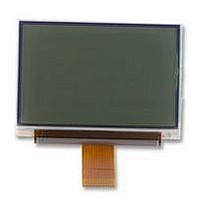
LCD MODULE, 128X64, LED B/L
Manufacturer
POWERTIP
Datasheet
1.PG12864LRF-NRA-H-Q.pdf
(29 pages)
Specifications of PG12864LRF-NRA-H-Q
Lcd Display Type
FSTN
Pixel Size (h X W)
0.28mm X 0.34mm
Viewing Area (h X W)
45.2mm X 27mm
Supply Voltage
3.3V
External Depth
6mm
External Length / Height
39mm
External
RoHS Compliant
Display Mode
Transflective


2-4.10 Increment Control Register Set
(iii) SWAP Command (For the Graphic Display only)
(iii) NLIN Command (For the Graphic Display only)
(iv) REV Command (For the Graphic Display only)
※ mark shows “Don’t care”(At the time of reset: (AIM, AY1, AX1)= 0H, read address :AH)
EXTERNAL DATA D7 D6 D5 D4 D3 D2 D1 D0 D7 D6 D5 D4 D3 D2 D1 D0
INTERNAL DATA
SWAP=”1”: Normal mode. In data-writing, the data of D7~D0 can be written to the
RE
REV=”0”: When RAM data at “H”, LCD at ON voltage (normal)
REV=”1”: When RAM data at “L”, LCD at ON voltage (reverse)
When data to the Graphic Display RAM are written, the write data are swapped.
0
Display RAM.
SWAP=”1”: SWAP mode ON. In data-writing, the swapped data of D7~D0 can be written to the
Graphic Display RAM.
The ON/OFF control of n-line alternated drive is performed.
NLIN=”0” : n line alternated drive OFF. By using frame cycle, the alternated signals (M)
are reversed.
NLIN=”1” : n line alternated drive ON. According to data set up in n line alternated register, the
alternation is made.
Corresponding to the data of the Graphic Display RAM, the lighting or not-lighting of the
display is set up.
The increment mode is set up when accessing to the Graphic Display RAM. (The Graphic
Display RAM only)
By AIM, AY1 and AX1 registers, the setting-up of increment operation /non-operation for the
X-address counter and the Y-address counter every write access of every read access to the
Graphic Display RAM is possible.
In setting to this control register, the increment operation of address can be made without setting
successive addresses for writing data or for reading data to the Graphic Display RAM from MPU.
After setting this register be sure to set the X and Y Address Register.
0
0
1
1
When REF=”1”,please set X address of Segment Display Circuits like below.
X ADDRESS
RS
1
00H->0FH
01H->0EH
H0E
00H
01H
0FH
D7
1
DISPLAY DEVICES FOR BETTER ELECTRONIC DESIGN
POWERTIP TECHNOLOGY CORPORATION
d7 d6 d5 d4 d3 d2 d1 d0
D6
0
D7(MSB)
D3(MSB)
D7(MSB)
D3(MSB)
D0(LSB)
D0(LSB)
D0(LSB)
D0(LSB)
D7~D0
SWAP=”0”
D5
1
X ADDRESS
D4
0
00H
01H
00H
01H
D3
※
d0 d1 d2 d3 d4 d5 d6 d7
D7(MSB)
D3(MSB)
D7(MSB)
D3(MSB)
D0(LSB)
D0(LSB)
D0(LSB)
D0(LSB)
D7-D0
AIM
SWAP=”1”
D2
AY1
D1
SEGS8->SEGS11
SEGS8->SEGS11
SEGS0->SEGS7
SEGS0->SEGS7
SEG OUTPUT
D7->D0
D0->D7
D0->D3
D0~D3
AX1
D0
Graphic
Related parts for PG12864LRF-NRA-H-Q
Image
Part Number
Description
Manufacturer
Datasheet
Request
R

Part Number:
Description:
POWERTIP
Manufacturer:
Powertip Technology
Datasheet:
Part Number:
Description:
POWERTIP
Manufacturer:
Powertip Technology
Datasheet:
Part Number:
Description:
Powertip
Manufacturer:
Powertip Technology Corp.
Datasheet:
Part Number:
Description:
POWERTIP DISPL DEVICES FOR BET
Manufacturer:
Powertip Technology
Datasheet:
Part Number:
Description:
POWERTIP
Manufacturer:
Powertip Technology
Datasheet:
Part Number:
Description:
POWERTIP
Manufacturer:
Powertip Technology
Datasheet:
Part Number:
Description:
STANDARD VALUE
Manufacturer:
POWERTIP [Powertip Technology]
Datasheet:
Part Number:
Description:
OUTLINE DIMENSION & BLOCK DIAGRAM
Manufacturer:
POWERTIP [Powertip Technology]
Datasheet:
Part Number:
Description:
OUTLINE DIMENSION & BLOCK DIAGRAM
Manufacturer:
POWERTIP [Powertip Technology]
Datasheet:
Part Number:
Description:
OUTLINE DIMENSION & BLOCK DIAGRAM
Manufacturer:
POWERTIP [Powertip Technology]
Datasheet:
Part Number:
Description:
POWERTIP
Manufacturer:
Powertip Technology
Datasheet:
Part Number:
Description:
STANDARD VALUE
Manufacturer:
POWERTIP [Powertip Technology]
Datasheet:
Part Number:
Description:
OUTLINE DIMENSION & BLOCK DIAGRAM
Manufacturer:
POWERTIP [Powertip Technology]
Datasheet:
Part Number:
Description:
OUTLINE DIMENSION & BLOCK DIAGRAM
Manufacturer:
POWERTIP [Powertip Technology]
Datasheet:
Part Number:
Description:
Standard Value
Manufacturer:
Powertip Technology
Datasheet: