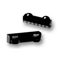
TFBS4650 Vishay, TFBS4650 Datasheet - Page 7

TFBS4650
Manufacturer Part Number
TFBS4650
Description
TRANSCEIVER, IRDA
Manufacturer
Vishay
Datasheet
1.TFBS4650.pdf
(13 pages)
Specifications of TFBS4650
Data Rate Max
115.2Kbps
Data Transmission Distance
30cm
Peak Wavelength
886nm
Supply Current
2mA
Supply Voltage Range
2.4V To 3.6V
Operating Temperature Range
-25°C To +85°C
Msl
MSL 4 - 72 Hours
External
RoHS Compliant
External Depth
1.6mm
Rohs Compliant
Yes
Communication Cone
15°
Svhc
No SVHC (20-Jun-2011)
Available stocks
Company
Part Number
Manufacturer
Quantity
Price
Company:
Part Number:
TFBS4650
Manufacturer:
YC
Quantity:
10 000
TFBS4650
Vishay Semiconductors
Recommended Circuit Diagram
Operated at a clean low impedance power supply the
TFBS4650 needs only one additional external com-
ponent when the IRED drive current should be mini-
mized for minimum current consumption according
the low power IrDA standard. When combined opera-
tion in IrDA and Remote Control is intended no cur-
rent limiting resistor is recommended.
However, depending on the entire system design and
board layout, additional components may be required
(see figure 1). When long wires are used for bench
tests, the capacitors are mandatory for testing rise/fall
time correctly.
The capacitor C1 is buffering the supply voltage V
and eliminates the inductance of the power supply
line. This one should be a small ceramic version or
other fast capacitor to guarantee the fast rise time of
the IRED current. The resistor R1 is necessary for
controlling the IRED drive current when the internally
controlled current is too high for the application.
Vishay transceivers integrate a sensitive receiver and
a built-in power driver. The combination of both needs
a careful circuit board layout. The use of thin, long,
resistive and inductive wiring should be avoided. The
inputs (TXD, SD) and the output RXD should be
directly (DC) coupled to the I/O circuit.
The capacitor C2 combined with the resistor R2 is the
low pass filter for smoothing the supply voltage.
As already stated above R2, C1 and C2 are optional
and depend on the quality of the supply voltages V
and injected noise. An unstable power supply with
dropping voltage during transmission may reduce the
sensitivity (and transmission range) of the trans-
ceiver.
The placement of these parts is critical. It is strongly
www.vishay.com
126
V
V
GND
SD
Txd
Rxd
Figure 1. Recommended Application Circuit
CC2
CC1
C1
R1
R2
C2
IRED Anode
IRED Cathode
V
Ground
SD
Txd
Rxd
CC
19286
CCx
cc2
recommended to position C2 as close as possible to
the transceiver power supply pins.
When connecting the described circuit to the power
supply, low impedance wiring should be used.
In case of extended wiring the inductance of the
power supply can cause dynamically a voltage drop
at V
follow the fast current is rise time. In that case another
10 µF cap at V
Keep in mind that basic RF-design rules for circuit
design should be taken into account. Especially
longer signal lines should not be used without termina-
tion. See e.g. "The Art of Electronics" Paul Horowitz,
Wienfield Hill, 1989, Cambridge University Press,
ISBN: 0521370957.
Table 2.
Recommended Application Circuit Components
Table 3.
Recommended resistor R1 [Ω]
Component
CC2
C1, C2
R1
R2
. Often some power supplies are not able to
V
2.7
3.0
3.3
[V]
CC2
CC2
will be helpful.
0.1 µF, Ceramic Vishay part#
47 Ω, 0.125 W (V
Minimized current consumption,
VJ 1206 Y 104 J XXMT
Recommended Value
IrDA Low power compliant
See table 3
Document Number 84672
24
30
36
Rev. 1.1, 03-Jul-06
CC1
= 3 V)


