AMMP-6408-TR1G Avago Technologies US Inc., AMMP-6408-TR1G Datasheet
AMMP-6408-TR1G
Specifications of AMMP-6408-TR1G


Related parts for AMMP-6408-TR1G


AMMP-6408-TR1G Summary of contents
Page 1
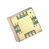
... GHz 1 W Power Amplifier in SMT Package Data Sheet Description The AMMP-6408 MMIC is a broadband 1W power amplifier in a surface mount package designed for use in transmitters that operate in various frequency bands between 6 GHz and 18 GHz GHz, it provides 29 dBm of output power (P-1dB) and small-signal gain from a small easy-to-use device ...
Page 2
Absolute Maximum Ratings Symbols Parameters Vd-Vg Drain to Gate Voltage Vd Positive Supply Voltage Vg Gate Supply Voltage Id Drain Current PD Power Dissipation Pin CW Input Power Tch Operating Channel Temp Tstg Storage Case Temp. Tmax Maximum Assembly Temp ...
Page 3
MTTF vs. Tchannel Temperature Operation 60% Confidence Level Tj λ (ФIT) MTTF (hrs) 150 3511 2.8E+05 140 1298 7.7E+05 130 456 2.2E+06 120 152 6.6E+06 110 48 2.1E+07 100 14 7.0E+ 2.5E+ 9.9E+ 4.2E+09 ...
Page 4
Typical Performances (Data Obtained from 3.5-mm Connector Based Test Fixture, and This Data is Including Connecter Loss, and Board Loss 25° 650 mA ...
Page 5
IM3 (dBc) Ids (mA) -20 -30 -40 -50 -60 -70 - SCL (dBm) Figure 7. Typical IM3 level and Ids vs. single carrier output level at 6 GHz 0 -10 ...
Page 6
S11_20 -20 S11_-40 S11_85 - FREQUENCY (GHz) Figure 13. Typical S11 over temperature 0 -5 -10 -15 S22_20 -20 S22_-40 S22_85 - FREQUENCY (GHz) Figure 15. Typical S22 ...
Page 7
Typical Scattering Parameters , (T A Freq S11 [GHz] dB Mag Phase 6 -3.83 0.64 -7.36 7 -4.33 0.61 -37.59 8 -4.35 0.61 -57.25 9 -2.87 0.72 -67.80 10 -2.18 0.78 -81.97 11 -1.88 0.81 -99.66 12 -2.85 0.72 ...
Page 8
... DC quiescent biasing condition at Vds = 5 V, Ids = 650 mA, Vgg = -1 V, typical gate terminal current is approximately 0.3mA active biasing technique is selected for the AMMP6408 MMIC PA DC biasing, the active biasing circuit must have more than 10-times higher internal current that the gate terminal current. ...
Page 9
800 μ 800 μ Figure 17. Simplified schematic for the MMIC die 800 μm 50 10K 50 800 μ ...
Page 10
RF INPUT -0 μF 100 pF 100 pF Note: 1. Vdd may be applied to either Pin 2 or Pin 6. 2. Vgg may be applied to either Pin 1 or Pin 7. ...
Page 11
... Recommended SMT Attachment for 5x5 Package The AMMP Packaged Devices are compatible with high volume surface mount PCB assembly processes. The PCB material and mounting pattern, as defined in the data sheet, optimizes RF performance and is strongly recommended. An electronic drawing of the land pattern is available upon request from Avago Sales & ...
Page 12
... Figure 1 will vary among different solder pastes from different manufacturers and is shown here for reference only. Ordering Information MELTING POINT = 218 C AMMP-6408 Part Number Ordering Information Part Number AMMP-6408-BLKG COOLING AMMP-6408-TR1G 200 250 300 AMMP-6408-TR2G 0.011 (0.28) 0.126 0.059 (3.2) (1 ...
Page 13
... For product information and a complete list of distributors, please go to our website: Avago, Avago Technologies, and the A logo are trademarks of Avago Technologies in the United States and other countries. Data subject to change. Copyright © 2005-2010 Avago Technologies. All rights reserved. Obsoletes AV02-0243EN AV02-2240EN - January 20, 2010 AMMP XXXX ∅1.55 ± 0.05 R 0.50 TYP. ...