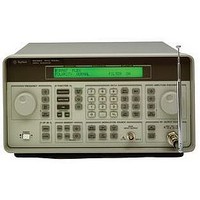
8648B AGILENT TECHNOLOGIES, 8648B Datasheet - Page 24

8648B
Manufacturer Part Number
8648B
Description
SIGNAL GENERATOR FREQUENCY / PULSE, 2GHZ
Manufacturer
AGILENT TECHNOLOGIES
Datasheet
1.8648B.pdf
(32 pages)
Specifications of 8648B
Signal Generator Type
Signal
Bandwidth
2GHz
Modulation Type
AM, FM, Phase
Supply Voltage Range
90V To 264V
External Height
165mm
External Width
330mm
External Depth
368mm
Lead Free Status / RoHS Status
na
24
User equipment (UE) setup
FIR filter
Chip rate
Primary scrambling code
Secondary scrambling offset
Uplink synchronization signal setup
Uplink channel configurations
Pre-set channel type
User defined channels
One DPCCH, one DPDCH, up to 6 transport channels
DPCCH (Dedicated Physical Control Channel)
Reference measurement channel: 12.2 kbps, 64 kbps, 144 kbps,
384 kbps
UDI 64 k
AMR 12.2 k
Power
Beta
Channel code
TFCI pattern
TFCI state
Symbol rate
FBI pattern
FBI state
Slot format
Interleaver
TPC pattern
TPC pattern steps
Root Nyquist, Nyquist
Gaussian
1 kcps to 4.25 Mcps
0 to 16777215
0 to 15
Timing offset range:
Synchronization signal
Frame clock interval
Frame clock polarity
SFN RST polarity
Sync trigger mode
External clock rate
External clock polarity
–40 to 0 dB
0 to 15 (coupled to power)
0 to 255
PN9, PN15, 0 to 03FF hex, user file
(Depends on slot format)
15 ksps (Non adjustable)
PN9, PN15, 0 to 3FFFFFFF hex, user file
(Depends on slot format)
0 to 5
On (non adjustable)
PN9, PN15, 4-bit repeating pattern,
user file, up/down, down/up, all up,
all down
1 to 80
a= 0 to 1
BbT= 0 to 1
Timing offset 512 to 2560 chips
Slot delay 0 to 119 slots
System Frame Number (SFN) reset
or frame clock
10 ms, 20 ms, 40 ms, 80 ms
Positive, negative
Positive, negative
Single, continuous
BBG data clock (chip clock) setup
internal, external
x 1 (3.84 MHz), x 2 (7.68 MHz)
x 4 (15.36 MHz)
Positive, negative
DPDCH (Dedicated Physical Data Channel)
Transport channel setup
Input
Output
Power
Beta
Channel code
Data
Symbol rate
Slot format
Block size
Number of blocks
Coding
TTI
Data
Rate matching attributes
CRC size
Error insertion
BLER (Block Error Rate)
BER (Bit Error Rate)
Bits frame
Synchronization signal (SFN RST or frame clock): Pattern trigger in
BBG data clock (chip clock): data clock in
Chip clock out (3.84 MHz): Data clock out
Frame timing out: system sync out
DPDCH (I) symbol data: event1 out
DPDCH (I) symbol clock: event2 out
DPCCH (Q) symbol data: data out
Off, –40 to 0 dB
0 to 15 (coupled to power)
0 to 255 (maximum value depends
on symbol rate/slot format)
PN9, PN15, 4-bit repeating pattern,
user file, transport channel
15, 30, 60, 120, 240, 480, 960 ksps
depending on slot format
0 to 6
0 to 5000
0 to 4095
1/2 convolutional, 1/3 convolutional,
turbo, none
10 ms, 20 ms, 40 ms, and 80 mSec
PN9, 4-bit repeating pattern, user file
1 to 256
0 to 1 (resolution 0.001)
0 to 1 (resolution 0.0001)
0, 8, 12, 16, 24
BLER or BER, or none
Automatically calculated


