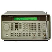
8648B AGILENT TECHNOLOGIES, 8648B Datasheet - Page 29

8648B
Manufacturer Part Number
8648B
Description
SIGNAL GENERATOR FREQUENCY / PULSE, 2GHZ
Manufacturer
AGILENT TECHNOLOGIES
Datasheet
1.8648B.pdf
(32 pages)
Specifications of 8648B
Signal Generator Type
Signal
Bandwidth
2GHz
Modulation Type
AM, FM, Phase
Supply Voltage Range
90V To 264V
External Height
165mm
External Width
330mm
External Depth
368mm
Lead Free Status / RoHS Status
na
General characteristics
Coherent carrier output
Outputs RF modulated with FM or M, but not IQ or AM. Nominal
power 0 dBm ±5 dB. Frequency range from 249.99900001 MHz to
maximum frequency. For RF carriers below this range, output
frequency = 1 GHz – frequency of RF output. Damage levels 20 V
and 13 dBm reverse RF power. (SMA, rear panel)
With ESG-DP and ESG-D series and
Option UN8 only
Data input
Accepts serial data for digital modulation applications. Expects
CMOS input. Leading edges must be synchronous with DATA
CLOCK rising edges. The data must be valid on the DATA CLOCK
falling edges. Damage levels are > +8 and < –4 V. (BNC, front panel)
Data clock input
Accepts CMOS clock signal (either bit or symbol), to synchronize
inputting serial data. Damage levels are > +8 and < –4 V. (BNC,
front panel)
Symbol sync input
Accepts CMOS synchronization signal. Symbol sync might occur
once per symbol or be a single, one bit wide pulse to synchronize
the first bit of the first symbol. Damage levels are > +8 and < –4 V.
(BNC, front panel)
Baseband generator reference input
Accepts 0 to +20 dBm sinewave, or TTL squarewave, to use as
reference clock for GSM applications. Only locks the internal
data generator to the external reference; the RF frequency is still
locked to the 10 MHz reference. Nominal impedance is 50 ohms at
13 MHz, AC-coupled. Damage levels are > +8 and < –8 V. (BNC,
rear panel)
Burst gate input
Accepts CMOS signal for gating burst power when externally sup-
plying data. Damage levels are > +8 and < –4 V. (BNC
Pattern trigger input accepts CMOS signal to trigger internal pat-
tern or frame generator to start single pattern output. Damage
levels are > + 8 and < –4 V. (BNC
Event 1 output
Outputs pattern or frame synchronization pulse for triggering or
gating external equipment. May be set to start at the beginning of a
pattern, frame, or timeslot and is adjustable to within ± one timeslot
with one bit resolution. Damage levels are > + 8 and < –4 V. (BNC
rear panel)
Event 2 output
Outputs data enable signal for gating external equipment.
Applicable when external data is clocked into internally generated
timeslots. Data is enabled when signal is low. Damage levels
> +8 and < –4 V. (BNC
Data output
Outputs data from the internal data generator or the externally
supplied signal at data input. CMOS signal. (BNC
Data clock output relays a CMOS bit clock signal for synchronizing
serial data. (BNC
Symbol sync output
Outputs CMOS symbol clock for symbol synchronization, one data
clock period wide. (BNC
1. Option 1EM replaces this BNC connector with an SMB connector.
1
, rear panel)
1
, rear panel)
1
, rear panel)
1
, rear panel)
(continued)
1
, rear panel)
1
, rear panel)
dc
1
,
"I" and "Q" baseband outputs
Outputs in-phase and quadrature-phase component of I/Q modula-
tion from the internal baseband generator. Full scale is 1 V
peak. Nominal impedance 50 ohms, DC-coupled, damage levels are
> +2 and < –2 V. (BNC, rear panel)
With ESG-DP and ESG-D series and
Option UND only
Baseband generator reference input
Accepts a TTL or > –10 dBm sinewave. Rate is 250 kHz to 20 MHz.
Pulse width is > 10 ns.
Trigger types Continuous, single, gated, segment advance
"I" and "Q" baseband outputs
Outputs in-phase and quadrature-phase component of I/Q modula-
tion from the internal baseband generator. Full scale is 1 V
peak. Nominal impedance 50 ohms, DC-coupled, damage levels are
> +2 and < –2 V. (BNC, rear panel)
Event 1 output
Even second output for multichannel CDMA. Damage levels are
> +8 V and < –4 V. (BNC
With ESG-DP and ESG-D series and
Option UN7 only
Data, clock and clock gate inputs
Accepts TTL or 75
30% to 70%. Damage levels are > +8 V and < –4 V (BNC
Sync loss output
Outputs a TTL signal that is low when sync is lost. Valid only when
measure end is high. Damage levels are > +8 V and < –4 V. (SMB,
rear panel)
No data detection output
Outputs a TTL signal that is low when no data is detected. Valid
only when measure end is high. (SMB, rear panel)
Error-bit-output (not supported at 10 Mbps rate)
Outputs 80 ns (typical) pulse when error bit is detected. (SMB, rear
panel)
Test result output
Outputs a TTL signal that is high for fail and low for pass. Valid only
on measure end falling edge. (SMB, rear panel)
Measure end output
Outputs a TTL signal that is high during measurement. Trigger
events are ignored while high. (SMB, rear panel)
With ESG-DP and ESG-D series and Option UNA
Alternate power input
Accepts CMOS signal for synchronization of external data and
alternate power signal timing. Damage levels are > +8 and < –4V.
(BNC
With ESG-D and Option 300
321.4 MHz input
Accepts a 321.4 MHz IF signal. Nominal input impedance 50 ohms.
(SMB, rear panel)
1
, rear panel)
input. Polarity is selected. Clock duty cycle is
1
, rear panel)
1
, rear panel)
peak
peak
to
to
29


