CX5032SB12000F0FLJZZ AVX Corporation, CX5032SB12000F0FLJZZ Datasheet - Page 26
CX5032SB12000F0FLJZZ
Manufacturer Part Number
CX5032SB12000F0FLJZZ
Description
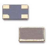
CRYSTAL, SM, CX-96F, 12MHZ
Manufacturer
AVX Corporation
Series
CX5032SBr
Datasheet
1.CX5032SB13000F0FLJZZ.pdf
(27 pages)
Specifications of CX5032SB12000F0FLJZZ
Operating Temperature Range
-30°C To +85°C
Crystal Mounting Type
SMD
Crystal Case Type
5
Frequency
12MHz
Frequency Tolerance
± 10ppm
Load Capacitance
10pF
Frequency Stability
± 10ppm
Lead Free Status / RoHS Status
Lead free / RoHS Compliant


(8) Excitation power of oscillation circuit
(9) Precautions for designing printed circuit board
R
which prevents increase in the load resonance resistance.
To prevent decrease in the negative resistance, connect the crystal unit to the base of the transistor as in the fundamental
mode crystal oscillation circuit. To use the crystal circuit for both oscillation and multiplication, connect a parallel resonance
circuit having multiplication frequency as resonance frequency to the collector of the transistor.
When selecting circuit constants for zero adjustment range by trimmer capacitor, set the constants to values obtained by
adding approx. 12 to 1510
measuring the crystal unit with load capacitances in series. (When the room temperature deviation specification of the crystal
unit is 1010
Normal operation of crystal units is not assured when excitation power is raised. The allowable excitation power varies
depending on the shape of the crystal unit or the stability of targeted frequency. When highly accurate oscillation is required,
however, it is recommended to use an oscillation circuit with an excitation power of 5 to 50 µW or less. For other cases, refer
to individual relevant crystal units on the pages of the catalog.
Be sure to design printed circuit board patterns that connect a crystal unit with other oscillation elements so that the lengths
of such patterns become shortest possible to prevent deterioration of characteristics due to stray capacitances and wiring
inductance. For multi-layer circuit boards, it is important not to wire the ground and other signal patterns right beneath the
oscillation circuit.
L
in the equation of load resonance resistance can be made equal to R
Handling Notes
-6
)
-6
to the room temperature deviation of the crystal unit, centering the value obtained by
L
1
C
1
R
C
1
t
R
L
R
1
R
- 59 -
R
3
1
2
C
C
0
L
C
1000P
C
C
2
4
2
3
S
Vcc
R
L
2
4
by connecting C
C
6
C
5
OUT
L
in series, or making it infinite,
Related parts for CX5032SB12000F0FLJZZ
Image
Part Number
Description
Manufacturer
Datasheet
Request
R

Part Number:
Description:
Manufacturer:
AVX Corporation
Datasheet:
Part Number:
Description:
Manufacturer:
AVX Corporation
Datasheet:
Part Number:
Description:
Manufacturer:
AVX Corporation
Datasheet:
Part Number:
Description:
Manufacturer:
AVX Corporation
Datasheet:
Part Number:
Description:
Manufacturer:
AVX Corporation
Datasheet: