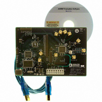
AD9957/PCBZ Analog Devices Inc, AD9957/PCBZ Datasheet - Page 38

AD9957/PCBZ
Manufacturer Part Number
AD9957/PCBZ
Description
D/A Converter Evaluation Board
Manufacturer
Analog Devices Inc
Series
AgileRF™r
Datasheet
1.AD9957BSVZ-REEL.pdf
(64 pages)
Specifications of AD9957/PCBZ
Silicon Manufacturer
Analog Devices
Application Sub Type
Direct Digital Synthesizer
Kit Application Type
Clock & Timing
Silicon Core Number
AD9957
Kit Contents
Board
Main Purpose
Timing: DDS Modulators
Embedded
No
Utilized Ic / Part
AD9957
Primary Attributes
14-Bit DAC, 32-Bit Tuning Word Width
Secondary Attributes
1GHz, Graphical User Interface
Lead Free Status / RoHS Status
Lead free / RoHS Compliant
Available stocks
Company
Part Number
Manufacturer
Quantity
Price
Company:
Part Number:
AD9957/PCBZ
Manufacturer:
LT
Quantity:
962
AD9957
Table 9. OSK Amplitude Step Size
ASF<1:0>
00
01
10
11
As mentioned earlier, the step interval is controlled by a 16-bit
programmable timer. Normally, this timer is loaded with the
programmed timing value whenever the timer expires, thus
initiating a new timing cycle. However, three events cause the
timer to have its timing value reloaded prior to the timer expiring.
One such event is when the Select Auto-OSK bit is transitioned
from a Logic 0 state to a Logic 1 state followed by an I/O update. A
second such event is a change of state in the OSK pin. The third
event is dependent on the status of the Load ARR @ I/O Update
bit. If this bit is Logic 0, no action occurs; otherwise, when the
I/O_UPDATE pin is asserted (or a profile change occurs), the
timer resets to its initial starting point.
PROFILES
Each of the three operating modes of the AD9957 support the
use of profiles, which consist of a group of registers containing
pertinent operating parameters for a particular operating mode.
Profiles enable rapid switching between parameter sets. Profile
parameters are programmed via the serial I/O port. Once pro-
grammed, a specific profile is activated by means of three
external pins (PROFILE<2:0>). A particular profile is activated
by providing the appropriate logic levels to the profile control
pins per the settings listed in Table 10.
Table 10. Profile Control Pins
PROFILE<2:0>
000
001
010
011
100
101
110
111
Consider an application of basic two-tone frequency shift
keying (FSK) where binary data is transmitted by selecting
between two different frequencies: a mark frequency (Logic 1)
and a space frequency (Logic 0). To accommodate FSK, the
Profile 0 register is programmed with the appropriate frequency
tuning word for a space, and the Profile 1 register is programmed
with the appropriate frequency tuning word for a mark. Then,
with the PROFILE1 and PROFILE2 pins tied to Logic 0, the
PROFILE0 pin is used to transmit the data bits. The logic state
of the PROFILE0 pin causes the appropriate mark and space
frequencies to be generated.
Amplitude Step Size
1
2
4
8
Active Profile
0
1
2
3
4
5
6
7
Rev. B | Page 38 of 64
I/O_UPDATE PIN
By default, the I/O_UPDATE pin is an input that serves as a
strobe signal to allow synchronous update of the device operating
parameters. For example, frequency, phase, and amplitude con-
trol words for the DDS can be programmed using the serial I/O
port. However, the serial I/O port is an asynchronous interface;
consequently, programming of the device operating parameters
using the I/O port is not synchronized with the internal timing.
Using the pin, I/O_UPDATE, the user can synchronize the
application of certain programmed operating parameters with
external circuitry when new parameters are programmed into
the I/O registers. A rising edge on I/O_UPDATE initiates transfer
of the register contents to the internal workings of the device.
The transfer of programmed data from the programming
registers to the internal hardware is also accomplished by
changing the state of the profile pins.
AUTOMATIC I/O UPDATE
The AD9957 offers an option whereby the I/O update function
is asserted automatically rather than relying on an external
signal supplied by the user. This feature is enabled by setting the
Internal I/O Update Active bit in CFR2.
When this feature is active, the I/O_UPDATE pin becomes an
output pin. It generates an active high pulse each time an inter-
nal I/O update occurs. The duration of the pulse is approximately
12 cycles of SYSCLK. This I/O update strobe can be used to
notify an external controller that the device has generated an
I/O update internally.
The repetition rate of the internal I/O update is programmed
via the serial I/O port. Two parameters control the repetition
rate. The first parameter consists of the two I/O update rate
control bits in CFR2. The second parameter is the 32-bit word
in the I/O update rate register that sets the range of an internal
counter.
The I/O update rate control bits establish a divide by 1, 2, 4, or 8
of a clock signal that runs at ¼ f
clocks the aforementioned 32-bit internal counter. The repetition
rate of the I/O update is given by
where:
A is the value of the 2-bit word comprising the I/O update rate
control bits.
B is the value of the 32-bit word stored in the I/O update rate
register.
If B is programmed to 0x0003 or less, the I/O_UPDATE pin no
longer pulses, but assumes a static Logic 1 state.
f
I
/
O
_
UPDATE
=
f
SYSCLK
2
A
B
SYSCLK
. The output of the divider


