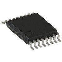
SI9118DB Vishay, SI9118DB Datasheet - Page 9

SI9118DB
Manufacturer Part Number
SI9118DB
Description
Pulse Width Modulation (PWM) Controller IC
Manufacturer
Vishay
Datasheet
1.SI9118DY-T1.pdf
(10 pages)
Specifications of SI9118DB
Silicon Manufacturer
Vishay
Application Sub Type
Pulse Width Modulation (PWM) Controller
Kit Application Type
Power Management
Silicon Core Number
SI9118
Kit Contents
Board
Lead Free Status / RoHS Status
Contains lead / RoHS non-compliant
DETAILED OPERATIONAL DESCRIPTION (CONT’D)
Programmable Duty Cycle Control
The maximum duty cycle limit is controlled by the volt-
age on D
80 % duty cycle while 0.0 V generates 0 % duty cycle.
The 80 % duty cycle is maximum default condition at
1 MHz switching frequency. The D
easily generated using resistor divider from the refer-
ence voltage.The maximum duty cycle limitation will be
different when the converter is synchronized by an
external frequency. If the internal free running frequency
is much slower than the external SYNC signal (SYNC
signal causes the internal clock to reset before the Cosc
voltage ramps to 3.2 V) , duty cycle is determined by the
one shot discharge time of the oscillator capacitor
(100 ns). Therefore, with 1 MHz SYNC signal, maximum
duty cycle of 90 % can be achieved (100 ns is 10 % of 1
MHz). If the internal free running frequency is very close
to the external SYNC frequency (SYNC signal causes
the internal clock to reset somewhere between 3.2 V to
4 V), duty cycle is determined by the ratio of C
at the SYNC point and the 3.2 V. At this condition, the
maximum duty cycle can be greater than 90 %. There-
fore, D
desired maximum duty cycle.
Slope Compensation
Slope compensation is necessary for duty cycles greater
than 50 % to stabilize the inner current loop and main-
tain overall loop stability. In order to simplify the slope
compensation circuitry, the Si9118 provides the buff-
ered oscillator ramp signal, V
slope compensation. V
high. The V
Vishay Siliconix maintains worldwide manufacturing capability. Products may be manufactured at one of several qualified locations. Reliability data for Silicon Tech-
nology and Package Reliability represent a composite of all qualified locations. For related documents such as package/tape drawings, part marking, and reliability
data, see http://www.vishay.com/ppg?70815.
Document Number: 70815
S-60550–Rev. D, 3-Apr-06
MAX
MAX
voltage must be modified in order to maintain
SC
pin. A D
signal super-imposed with actual current
MAX
SC
is only available when DR is
voltage of 3.2 V generates
SC
to be used for external
MAX
voltage can be
osc
voltage
sense signal should be used by the PWM comparator to
determine the duty cycle. The summation of this signal
should be fed into I
proper slope compensation is required. The amount of
slope compensation is determined by the resistors con-
nected to the I
same as the C
use with SYNC pin, instead of V
still operate at duty cycles greater than 50 % by gener-
ating an external slope compensation ramp using a
simple RC circuit from the MOSFET driver output pin as
shown on the application circuit.
Over Current Protection
Si9118/Si9119 are designed with a pulse-to-pulse peak
current limiting protection circuit to protect itself, and the
load in case of a failure. The voltage across the sense
resistor is monitored continuously and if the voltage
reaches its trigger level, the duty cycle is terminated.
This limits the maximum current delivered to the load. In
order to improve the accuracy of over current protection
from traditional controllers, Si9118/Si9119 are designed
with separate I
pin does not sum in the traditional slope compensation
voltage, which adds error into the detection level. I
is used to sum the current sense signal and the slope
compensation for loop stability.
Output Driver Stage
The DR pin is designed to drive a low-side N-Channel
MOSFET. The driver stage is sized to sink and source
peak currents up to 500 mA with V
vides ample drive capability for 50 W of output power.
CS
OSC
LIMIT
pin. The amplitude of the V
pin voltage (≈ 4 V). For designs which
CS
and I
Vishay Semiconductors
pin. For optimum performance,
CS
pins. Voltage on the I
SC
Si9118/Si9119
pin, the converter can
CC
= 12 V. This pro-
www.vishay.com
SC
signal is
CS
LIMIT
pin
9


