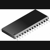
SI9130DB Vishay, SI9130DB Datasheet - Page 8

SI9130DB
Manufacturer Part Number
SI9130DB
Description
Pulse Width Modulation (PWM) Controller IC
Manufacturer
Vishay
Datasheet
1.SI9130CG.pdf
(14 pages)
Specifications of SI9130DB
Silicon Manufacturer
Vishay
Application Sub Type
Pin-programmable Controller
Kit Application Type
Power Management
Silicon Core Number
SI9130
Kit Contents
Board
Lead Free Status / RoHS Status
Contains lead / RoHS non-compliant
Si9130
Vishay Siliconix
DESCRIPTION OF OPERATION
The Si9130 is a dual step-down converter, which takes a 5.5-V
to 30-V input and supplies power via two PWM controllers (see
Figure 1). These 5-V and 3.3-V supplies run on an optional
300-kHz or 200-kHz internal oscillator, or an external sync
signal. Amount of output current is limited by external
components, but can deliver greater than 6 A on either supply.
As well as these two main Buck controllers, additional loads
can be driven from two micropower linear regulators, one 5 V
(V
are each rated to deliver 5 mA. If the linear regulator circuits fall
out of regulation, both Buck controllers are shut down.
www.vishay.com
8
+3.3 V at 3 A
L
Note 1: Use short, Kelvin-connected PC board
) and the other 3.3 V (REF)—see Figure 2. These supplies
150 mF
5.5 V to 30 V
traces placed very close to one another.
C7
INPUT
150 mF
C12
+3.3 V ON/OFF
+5 V ON/OFF
SHUTDOWN
OSC SYNC
25 mW
R1
22 mF
C1
D1FS4
(Note 1)
10 mH
D1
L1
0.01 mF
N1
N3
3.45ADJ
C9
OPEN
OPEN
GND
1N4148
0.1 mF
D2A
C5
FIGURE 1. Si9130 Application Circuit
Voltage Selection Table
Input
C3
1 mF
23
25
27
26
24
28
13
12
10
11
1
2
3
9
100 W
V+
BST
DH
LX
DL
CS
FB
SS
ON
ON
SHDN
SYNC
GND
REF
3.6ADJ
3
3
3
3
3
3
3
5
0.1 mF
OPEN
OPEN
Si9130
3
GND
3.45ADJ
3.6ADJ
PGND
BST
DH
CS
FB
SS
DL
LX
V
5
5
5
L
5
5
5
5
3.3-V PWM Voltage Selection
(Pins 3.45ADJ, 3.6ADJ)
The voltage at this output can be selected to 3.3 V, 3.45 V or
3.6 V, depending on the configuration of pins 3.45ADJ and
3.6ADJ. Leaving both pins open results in 3.3V nominal
output. Grounding pin 3.45ADJ while leaving 3.6ADJ open
delivers 3.45-V nominal output. Grounding 3.6 ADJ while
leaving 3.45ADJ open sets a 3.6-V nominal output.
22
18
16
17
19
15
21
14
20
8
7
0.1 mF
D2B
1N4148
Output
C4
3.45 V
FB
3.3 V
3.6 V
3
C8
0.01 mF
N2
N3
(Note 1)
10 mH
3.45-V Voltage Adjust
3.6-V Voltage Adjust
+3.3 V at 5 mA
L2
D1
D1FS4
25 mW
C10
22 mF
4.7 mF
R2
+5 V at 5 mA
C6
330 mF
S-40805—Rev. F, 26-Apr-04
+5 V at 3 A
Document Number: 70190


