ATJTAGICE2 - JMS2206 Atmel, ATJTAGICE2 - JMS2206 Datasheet - Page 3
ATJTAGICE2 - JMS2206
Manufacturer Part Number
ATJTAGICE2 - JMS2206
Description
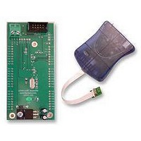
TEST BOARD KIT, COMBO
Manufacturer
Atmel
Datasheet
1.ATJTAGICE2_-_JMS2206.pdf
(5 pages)
Specifications of ATJTAGICE2 - JMS2206
Svhc
No SVHC (15-Dec-2010)
Development Tool Type
Development Kit
Kit Features
Supports Debugging With AVR Traditional JTAG Interface And With DebugWIRE Interface
Mcu Supported Families
AVR Microcontroller
Silicon Manufacturer
Atmel
Core Architecture
AVR
Core Sub-architecture
AVR UC3
Kit Contents
Board
Features
Integral 5-volt Linear Regulator, LED DC On Indicator
Rohs Compliant
Yes
Lead Free Status / RoHS Status
Lead free / RoHS Compliant


Connecting to the target through the ISP Interface
Re-enabling the ISP interface
Connecting to the target through the JTAG interface
2562C–AVR–07/06
Connecting to the ISP interface is described in the section documenting the debugWIRE
connection.
When the DWEN fuse is enabled the ISP interface is disabled in order to have full con-
trol over the RESET pin. Enabling the ISP interface again will disable the debugWIRE
interface:
1. Connect the JTAGICE mkII to the target ISP header.
2. From within a debug session, open "JTAGICE mkII Options" found in the
3. Click on the button "disable debugWIRE". Now the ISP interface is enabled and
At least 6 wires are required to connect the JTAGICE mkII to the target application.
These signals are TCK, TDO, TDI, TMS, VTref and GND.
Optional line is the nSRST. The nTRST signal is not used, and is reserved for compati-
bility with other equipment.
nSRST is used to control and monitor the target reset line - this is not necessary for cor-
rect emulation. However if the application code sets the JTD bit in the MCUCSR, the
JTAG interface will be disabled. In order for the JTAGICE mkII to be able to re-program
the target AVR, it will need to have control of the RESET Pin. Note that the nSRST line
is pulled high internally by a 10 KΩ load.
Figure 3 and Table 2 on page 4 show which JTAG lines should be connected to the tar-
get AVR to ensure correct operation. To avoid drive contention on the signal lines it is
recommended that series resistors are placed between the JTAG lines and any external
circuitry. The value of the resistor should be chosen so that the external circuitry and the
AVR do not exceed their maximum ratings (i.e. sink or source too much current).
Figure 3. JTAG10PIN connector
“Debug”-menu in AVR Studio and select the "Connections" tab
debugWIRE interface disabled.
TDO
TMS
TCK
TDI
1
2
GND
VTref
nSRST
(nTRST)
GND
AVR JTAGICE mkII
3
Related parts for ATJTAGICE2 - JMS2206
Image
Part Number
Description
Manufacturer
Datasheet
Request
R

Part Number:
Description:
AVR ON-CHIP D-BUG SYSTEM
Manufacturer:
Atmel
Datasheet:

Part Number:
Description:
JTAG EMULATOR FOR AVR
Manufacturer:
Atmel
Datasheet:

Part Number:
Description:
DEV KIT FOR AVR/AVR32
Manufacturer:
Atmel
Datasheet:

Part Number:
Description:
INTERVAL AND WIPE/WASH WIPER CONTROL IC WITH DELAY
Manufacturer:
ATMEL Corporation
Datasheet:
Part Number:
Description:
Low-Voltage Voice-Switched IC for Hands-Free Operation
Manufacturer:
ATMEL Corporation
Datasheet:
Part Number:
Description:
MONOLITHIC INTEGRATED FEATUREPHONE CIRCUIT
Manufacturer:
ATMEL Corporation
Datasheet:
Part Number:
Description:
AM-FM Receiver IC U4255BM-M
Manufacturer:
ATMEL Corporation
Datasheet:
Part Number:
Description:
Monolithic Integrated Feature Phone Circuit
Manufacturer:
ATMEL Corporation
Datasheet:
Part Number:
Description:
Multistandard Video-IF and Quasi Parallel Sound Processing
Manufacturer:
ATMEL Corporation
Datasheet:
Part Number:
Description:
High-performance EE PLD
Manufacturer:
ATMEL Corporation
Datasheet:
Part Number:
Description:
8-bit Flash Microcontroller
Manufacturer:
ATMEL Corporation
Datasheet:
Part Number:
Description:
2-Wire Serial EEPROM
Manufacturer:
ATMEL Corporation
Datasheet: