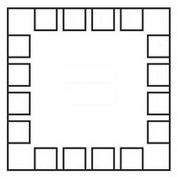
LDS8865002-T2-200/200/200 Leadis Technology, LDS8865002-T2-200/200/200 Datasheet

LDS8865002-T2-200/200/200
Specifications of LDS8865002-T2-200/200/200
Related parts for LDS8865002-T2-200/200/200
LDS8865002-T2-200/200/200 Summary of contents
Page 1
... LEDs. The ultra low dropout PowerLite Current Regulator increases device’s efficiency up to 94%. TYPICAL APPLICATION CIRCUIT © 2007 Leadis Technology Characteristics subject to change without notice The PWM1/PWM2 logic inputs function as a chip enable and a PWM mode LED brightness control. ...
Page 2
... PWM2 High Logic Level pins Low PWM frequency PWM duty cycle Thermal Shutdown Thermal Hysteresis Under Voltage Lockout (UVLO) Threshold Over Voltage Protection © 2007 Leadis Technology Characteristics subject to change without notice Rating Unit Vin + 0.7V V -65 to +160 °C -40 to +125 ° ...
Page 3
... LEDs at 20mA), C OUT Efficiency vs. Input Voltage Switching Frequency vs. Temperature Power-Up in 1.5x Mode Ch1 – PWM, PWM2, Ch2 – Vout, Ch3 – Output current (100mA/div) © 2007 Leadis Technology Characteristics subject to change without notice = 0.22 μ 1μ 25°C unless otherwise specified ...
Page 4
... Ch3 – Output current (AC coupled 20mA/div) Switching Waveforms at 1kHz PWM mode Ch1 – PWM, PWM2, Ch2 – Vout, Ch3 – Output current (100mA/div) © 2007 Leadis Technology Characteristics subject to change without notice Operating Waveforms in 1x Mode) Ch1 – Vin (AC coupled), Ch2 – Vout (AC coupled), Ch3 – ...
Page 5
... LDS8865 Switching Waveforms at 50kHz PWM mode Ch1 – PWM, PWM2, Ch2 – Vout, Ch3 – Output current (100mA/div) © 2007 Leadis Technology Characteristics subject to change without notice Switching Waveforms at 100kHz PWM mode Ch1 – PWM, PWM2, Ch2 – Vout, Ch3 – Output current (100mA/div) 5 Doc ...
Page 6
... Vout is the charge pump output that is connected to the LED anodes. A small 1 μ F ceramic bypass © 2007 Leadis Technology Characteristics subject to change without notice Function capacitor is required between the Vout pin and ground near the device. GND is the ground reference for the charge pump. ...
Page 7
... This sequence repeats at every mode until driver enters the 2x mode. © 2007 Leadis Technology Characteristics subject to change without notice Figure 2. LDS8865 Functional Block Diagram If the device detects a sufficient input voltage is present to drive all LED currents in 1x mode, it will change automatically back to 1x mode ...
Page 8
... OUT enabled, input current may increase up to 200 – 300 mA within 20 µs after enable and is limited to 35 – after that. © 2007 Leadis Technology Characteristics subject to change without notice 4. Over-Temperature Protection If the die temperature exceeds +150°C, the driver will enter shutdown mode. The LDS8868 requires restart after die temperature falls below 130° ...
Page 9
... LDS8865 ground plane underneath. The use of multiple via improves the package heat dissipation. Figure 4. Recommended layout © 2007 Leadis Technology Characteristics subject to change without notice 9 Doc. No. 8865DS, Rev. 2 ...
Page 10
... L 0.325 0.375 m 0.150 typ n 0.225 typ Note: 1. All dimensions are in millimeters 2. Complies with JEDEC Standard MO-220 © 2007 Leadis Technology Characteristics subject to change without notice MAX 0.80 0.05 0.228 0.30 3.05 1.75 3.05 1.75 0.425 10 Doc. No. 8865DS, Rev. 2 ...
Page 11
... The device used in the above example is a LDS8865 002–T2 (3x3 TQFN, Tape & Reel, 32/25/10.5 mA maximum current per LED bank 4) For additional package and temperature options, please contact your nearest Leadis Technology Sales office. © 2007 Leadis Technology Characteristics subject to change without notice ...
Page 12
... Leadis Technology products are not designed, intended, or authorized for use as components in systems intended for surgical implant into the body, or other applications intended to support or sustain life, or for any other application in which the failure of the Leadis Technology product could create a situation where personal injury or death may occur. Leadis Technology reserves the right to make changes to or discontinue any product or service described herein without notice. Products with data sheets labeled " ...


