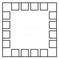
LDS8869002-T2 Leadis Technology, LDS8869002-T2 Datasheet

LDS8869002-T2
Specifications of LDS8869002-T2
Related parts for LDS8869002-T2
LDS8869002-T2 Summary of contents
Page 1
... LEDs. Inclusion of a 1.33x fractional charge pump mode and ultra low dropout PowerLite™ Current Regulator (PCR) increases TYPICAL APPLICATION CIRCUIT © 2008 Leadis Technology Characteristics subject to change without notice device’s efficiency up to 94%. New mode requires no additional external capacitors. ...
Page 2
... Transition Filter Delay Input Leakage EN/SET Pin High Logic Level Low Thermal Shutdown Thermal Hysteresis Under Voltage Lockout (UVLO) Threshold Over Voltage Protection Note: 1. Sample test only © 2008 Leadis Technology Characteristics subject to change without notice Rating Unit 0. -65 to +160 °C -40 to +125 ° ...
Page 3
... Reg2 should be empty to prevent data interference. Table 2. Reg1 Code Data Reg1 Bit Data pulses pulses Note: If bits Bit0 – Bit2 are set to zero, the corresponding LED bank is disabled. © 2008 Leadis Technology Characteristics subject to change without notice Conditions Description Bits Return Lockout 1 Reg1 Bit Data pulses ...
Page 4
... Leadis Technology Characteristics subject to change without notice LED Current, Data Reg2-5 value mA, IMODE = 1 Pulses (binary) 33 0.5 011111 34 32 011110 35 31.5 011101 31.0 36 011100 37 30.5 011011 30 38 ...
Page 5
... LDS8869 PROGRAMMING EXAMPLES Programming 6 LEDs to 32mA Programming 6 LED to 1mA © 2008 Leadis Technology Characteristics subject to change without notice 5 Doc. No. 8869_DS, Rev. 2.1 ...
Page 6
... LEDs at 20mA), C OUT Efficiency vs. Input Voltage Power-Up in 1.33x Mode EN/SET V OUT ILED 100mA/div Power- Mode EN/SET V OUT ILED 100mA/div © 2008 Leadis Technology Characteristics subject to change without notice = 0.22 μ 1μ 25°C unless otherwise specified OUT AMB EN/SET V OUT ILED ...
Page 7
... LDS8869 Operating Waveforms in 1x Mode OUT ILED 100mA/div Operating Waveforms in 1.5x Mode OUT ILED 100mA/div © 2008 Leadis Technology Characteristics subject to change without notice Operating Waveforms in 1.33x Mode OUT ILED 100mA/div Operating Waveforms in 2x Mode OUT ILED 100mA/div 7 Doc. No. 8869_DS, Rev. 2.1 ...
Page 8
... V is the charge pump output that is connected to OUT the LED anodes. A small 1 μ F ceramic bypass © 2008 Leadis Technology Characteristics subject to change without notice Function capacitor is required between the Vout pin and μ F ground near the device. GND is the ground reference for the charge pump. ...
Page 9
... If the input voltage is insufficient or falls to a level where Vd ≤75 mV, and the regulated currents cannot be maintained, the low dropout PowerLite™ Current © 2008 Leadis Technology Characteristics subject to change without notice Figure 2. LDS8869 Functional Block Diagram Regulator switches the charge pump into 1.33x mode ...
Page 10
... REG3, REG4, REG5 allow to set the current respectively in banks C, B and A. The three banks can be programmed with independent current values. © 2008 Leadis Technology Characteristics subject to change without notice REG6 contains the return lockout (RTLKO) bit. This stops the charge pump returning to 1x mode. One pulse sets ...
Page 11
... IN OUT citors (C1 and C2) X5R or X7R type. Capacitors C1 and C2 may be increased µF to improve © 2008 Leadis Technology Characteristics subject to change without notice charge pump efficiency by 3%. In all charge pump modes, the input current ripple is very low, and an input bypass capacitor of 1µF is sufficient. ...
Page 12
... L 0.325 0.375 m 0.150 typ n 0.225 typ Note: 1. All dimensions are in millimeters 2. Complies with JEDEC Standard MO-220 © 2008 Leadis Technology Characteristics subject to change without notice MAX 0.80 0.05 0.228 0.30 3.05 1.75 3.05 1.75 0.425 12 Doc. No. 8869_DS, Rev. 2.1 ...
Page 13
... The standard lead finish is Matte-Tin. 3) The device used in the above example is a LDS8869 002–T2 ( 3x3 TQFN, Tape & Reel). 4) For additional package and temperature options, please contact your nearest Leadis Technology Sales office. © 2008 Leadis Technology Characteristics subject to change without notice Package ...
Page 14
... Leadis Technology products are not designed, intended, or authorized for use as components in systems intended for surgical implant into the body, or other applications intended to support or sustain life, or for any other application in which the failure of the Leadis Technology product could create a situation where personal injury or death may occur. Leadis Technology reserves the right to make changes to or discontinue any product or service described herein without notice. Products with data sheets labeled " ...


