ADNS-6010 Avago Technologies US Inc., ADNS-6010 Datasheet
ADNS-6010
Specifications of ADNS-6010
Available stocks


Related parts for ADNS-6010


ADNS-6010 Summary of contents
Page 1
... This sensor is powered for the extremely high sensitive user There are no moving parts, in the complete assembly for ADNS-6010 laser mouse system, thus it is high reliability and less maintenance for the end user. In addition, preci- sion optical alignment is not required, facilitating high volume assembly ...
Page 2
Pinout Pin Name Description 1 NCS Chip select (active low input) 2 MISO Serial data output (Master In/Slave Out) 3 SCLK Serial clock input 4 MOSI Serial data input (Master Out/Slave In Connection 6 RESET Reset input ...
Page 3
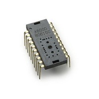
Figure 2. Package outline drawing CAUTION advised that normal static precautions be taken in handling and assembly of this component to prevent damage and/or degradation which may be induced by ESD 3 ...
Page 4
... Overview of Laser Mouse Sensor Assembly Figure 3. Assembly drawing of ADNS-6010 (top, front and cross-sectional view) 4 ...
Page 5
... The ADNS-6120 or ADNS-6130-001 Laser Mouse Lens is designed for use with ADNS-6010 sensor and the illumi- nation subsystem provided by the VCSEL assembly clip and the VCSEL. Together with the VCSEL, the ADNS-6120 ...
Page 6
Assembly Recommendation 1. Insert the sensor and all other electrical components into the application PCB (main PCB board and VCSEL PCB board). 2. Wave solder the entire assembly in a no-wash solder process utilizing a solder fixture. The solder fixture ...
Page 7
... Design considerations for improving ESD Performance For improved electrostatic discharge performance, typical creepage and clearance distance are shown in the table below. Assumption: base plate construction as per the Avago Technologies supplied IGES file and ADNS- 6130-001 trim lens (or ADNS-6120 round lens). SENSOR LENS BASE PLATE Figure 6 ...
Page 8
... NC pins should not be connected to any traces. x Surface mount parts are recommended. x Care must be taken when interfacing a 5V microcontroller to the ADNS-6010. Serial port inputs on the sensor should be con- nected to open-drain outputs from the microcontroller or use an active drive level shifter. NPD and RESET should be connected to 5V microcontroller outputs through a resistor divider or other level shifting technique ...
Page 9
... Avago Technologies recommends using the exact Rbin value specified in the bin table to ensure sufficient laser power for navigation. The system com- prised of the ADNS-6010 and ADNV-6340 is designed to maintain the output beam power within Class 1 require- ments over component manufacturing tolerances and ...
Page 10
... Single Fault Detection ADNS-6010 is able to detect a short circuit, or fault, condition at the RBIN and XY_LASER pins, which could lead to excessive laser power output. A low resistance path to ground on either of these pins will trigger the fault detection circuit, which will turn off the laser drive current source and set the LASER_NEN output high ...
Page 11
Absolute Maximum Ratings Parameter Symbol Storage Temperature T S Operating Temperature T A Lead Solder Temp Supply Voltage V DD3 ESD Input Voltage V IN Output current I OUT Input Current I IN Recommended Operating Conditions Parameter Symbol Operating Temperature ...
Page 12
AC Electrical Specifications Electrical Characteristics over recommended operating conditions. Typical values at 25 °C, V Parameter Symbol Min. VDD to RESET t OP Data delay after t PU-RESET RESET Input delay after T IN-RST reset Power Down t PD Wake ...
Page 13
DC Electrical Specifications Electrical Characteristics over recommended operating conditions. Typical values at 25 °C, V Parameter Symbol DC Supply Current I DD_AVG Power Down Supply I DDPD Current Input Low Voltage V IL Input High Voltage V IH Input hysteresis ...
Page 14
Typical Performance Characteristics Typical Resolution vs. Z 2400 2000 1600 1200 800 400 0 1.5 1.6 1.7 1.8 1.9 2.0 2.1 2.2 2.3 2.4 2.5 2.6 2.7 2.8 2.9 3.0 3.1 3.2 3.3 Distance from Lens Refremce Plane to Surface, ...
Page 15
... Figure 15. Relative Responsivity Synchronous Serial Port The synchronous serial port is used to set and read pa- rameters in the ADNS-6010, and to read out the motion information. The serial port is also used to load PROM data into the ADNS-6010. The port is a four wire port. The host micro-controller al- ways initiates communication ...
Page 16
... NOTE: The 250 ns minimum high state of SCLK is also the minimum MISO data hold time of the ADNS-6010. Since the falling edge of SCLK is actually the start of the next read or write command, the ADNS-6010 will hold the state of data on MISO until the falling edge of SCLK. 5 ...
Page 17
... SCLK rising edge of the last data bit of the previ- ous read operation. In addition, during a read operation SCLK should be delayed after the last address data bit to ensure that the ADNS-6010 has time to prepare the requested data. Burst Mode Operation Burst mode is a special serial port operation mode which may be used to reduce the serial transaction time for three predefi ...
Page 18
... Motion Read Reading the Motion_Burst register activates this mode. The ADNS-6010 will respond with the contents of the Motion, Delta_X, Delta_Y, SQUAL, Shutter_Upper, Shut- ter_Lower, and Maximum_Pixel registers in that order. After sending the register address, the micro-control- ler must wait t and then begin reading data. ...
Page 19
Frame Capture This is a fast way to download a full array of pixel values from a single frame. This mode disables navigation and overwrites any downloaded firmware. A hardware reset is required to restore navigation, and the firmware must ...
Page 20
... ESD events, power supply droops or micro-controller firmware flaws. In such a case, the micro-controller should pulse NCS high for at least 1 ms. The ADNS-6010 will reset the serial port (but not the control registers) and will be prepared for the beginning of a new transmission after the normal transaction delay ...
Page 21
... Notes on Power-up and the serial port Reset Circuit The ADNS-6010 does not perform an internal power up self-reset; the reset pin must be raised and lowered to reset the chip. This should be done every time power is applied. During power-up there will be a period of time after the power supply is high but before any clocks are available ...
Page 22
... Registers The ADNS-6010 registers are accessible via the serial port. The registers are used to read motion data and status as well as to set the device configuration. Address Register 0x00 Product_ID 0x01 Revision_ID 0x02 Motion 0x03 Delta_X 0x04 Delta_Y 0x05 SQUAL 0x06 ...
Page 23
... Field PID PID 7 6 Data Type: 8-Bit unsigned integer USAGE: This register contains a unique identification assigned to the ADNS-6010. The value in this register does not change; it can be used to verify that the serial communications link is functional. Revision_ID Access: Read Bit 7 6 Field ...
Page 24
Motion Access: Read Bit 7 6 Field MOT Reserved Data Type: Bit field. USAGE: Register 0x02 allows the user to determine if motion has occurred since the last time it was read. If so, then the user should read registers ...
Page 25
Delta_X Access: Read Bit 7 6 Field Data Type: Eight bit 2’s complement number. USAGE: X movement is counts since last report. Absolute value is determined by resolution. Reading clears the reg- ister. -128 -127 Motion ...
Page 26
SQUAL Access: Read Bit 7 6 Field Data Type: Upper 8 bits of a 10-bit unsigned integer. USAGE: SQUAL (Surface Quality measure of ¼ of the number of valid features visible by the sensor ...
Page 27
Pixel_Sum Access: Read Bit 7 6 Field Data Type: High 8 bits of an unsigned 16-bit integer. USAGE: This register is used to find the average pixel value. It reports the upper byte of a 16-bit ...
Page 28
Configuration_bits Access: Read/Write Bit 7 6 Field 0 LASER_MODE Data Type: Bit field USAGE: Register 0x0a allows the user to change the configuration of the sensor. Shown below are the bits, their default values, and optional values. Field Name Description ...
Page 29
Extended_Config Access: Read/Write Bit 7 6 Field Busy Reserved Data Type: Bit field USAGE: Register 0x0b allows the user to change the configuration of the sensor. Shown below are the bits, their default values, and optional values. Field Name Description ...
Page 30
Data_Out_Lower Access: Read Bit 7 6 Field Data_Out_Upper Access: Read Bit 7 6 Field Data Type: Sixteen bit word USAGE: Data in these registers come from the system self test or the ...
Page 31
Shutter_Lower Access: Read Bit 7 6 Field Shutter_Upper Access: Read Bit 7 6 Field Data Type: Sixteen bit unsigned integer. USAGE: Units are clock cycles. Read Shutter_Upper first, then Shutter_Lower. They should ...
Page 32
Mean Shutter vs. Z (White Paper) 2000dpi, Circle@7.5" diameter, Speed-6ips 200 180 160 140 120 100 -0.8 -0.6 -0.4 -0.2 Distance from Lens Reference Plane to Surface, Z (mm) Figure 30. Mean Shutter vs. Z ...
Page 33
Frame_Period_Lower Access: Read Bit 7 6 Field Frame_Period_Upper Access: Read Bit 7 6 Field Data Type: Sixteen bit unsigned integer. USAGE: Read these registers to determine the current frame period and to ...
Page 34
Frame_Capture Access: Read/Write Bit 7 6 Field Data Type: Bit field. USAGE: Writing 0x83 to this register will cause the next available complete 1 2/3 frames of pixel values to be stored to SROM RAM. Writing ...
Page 35
Configuration II Access: Read/Write Bit 7 6 Field Reserved Reserved Data Type: Bit field USAGE: Write to this register Field Name Description BIT 2 Must be set to one Force_disable 0 = LASER_NEN functions as normal 1 = LASER_NEN output ...
Page 36
Frame_Period_Max_Bound_Lower Access: Read/Write Bit 7 6 Field FBM FBM 7 6 Frame_Period_Max_Bound_Upper Access: Read/Write Bit 7 6 Field FBM FBM 15 14 Data Type: 16-bit unsigned integer. USAGE: This value sets the maximum frame period (the MINIMUM frame rate) which ...
Page 37
Frame_Period_Min_Bound_Lower Access: Read/Write Default Value: 0x7E Bit 7 6 Field FBm FBm 7 6 Frame_Period_Min_Bound_Upper Address: 0x1C Access: Read/Write Default Value: 0x0E Bit 7 6 Field FBm FBm 15 14 Data Type: 16-bit unsigned integer. USAGE: This value sets the ...
Page 38
Shutter_Max_Bound_Lower Access: Read/Write Bit 7 6 Field Shutter_Max_Bound_Upper Access: Read/Write Bit 7 6 Field Data Type: 16-bit unsigned integer. USAGE: This value sets the maximum allowable shutter value when operating in automatic ...
Page 39
LP_CFG0 Access: Read/Write Bit 7 6 Field Match LP 6 Data Type: 8-bit unsigned integer USAGE: This register is used to set the laser current and bin matching parameter used together with register 0x2D where register ...
Page 40
Reserved Address: 0x2f-0x3C Observation Access: Read/Write Bit 7 6 Field OB Reserved 7 Data Type: Bit field USAGE: Each bit is set by some process or action at regular intervals, or when the event occurs. The user must clear the ...
Page 41
... Data Type: Eight bit unsigned integer USAGE: The SROM_Load register is used for high-speed programming of the ADNS-6010 from an external PROM or microcontroller. See the Synchronous Serial Port section for use details. For product information and a complete list of distributors, please go to our web site: Avago, Avago Technologies, and the A logo are trademarks of Avago Technologies in the United States and other countries. Data subject to change. Copyright © ...